|
|
• 15 kV/µs minimum common mode transient immunity at VCM = 1500 V (4503/0453)
|
• High speed: 1 Mb/s
|
• TTL compatible
|
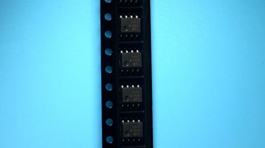
• Available in 8-Pin DIP, SO-8, widebody packages
|
• Open collector output
|
• Guaranteed performance from temperature: 0°C to70°C
|
|
| CATALOG |
HCPL-0452-500E PARAMETRIC INFO
|
HCPL-0452-500E PACKAGE INFO
|
HCPL-0452-500E MANUFACTURING INFO
|
HCPL-0452-500E PACKAGING INFO
|
HCPL-0452-500E APPLICATIONS
|
|
PARAMETRIC INFO
|
| Maximum Propagation Delay Time (tPHL) (ns) |
800 |
| Maximum Propagation Delay Time (tPLH) (ns) |
800 |
| Minimum Common Mode Rejection (kV/us) |
1(Typ) |
| Common Mode Voltage (V) |
10 |
| Typical Bandwidth (MHz) |
9 |
| Input Type |
DC |
| Output Type |
DC |
| Output Device |
Transistor With Base |
| Standard |
CSA|DIN|EN|UL|VDE |
| Number of Channels per Chip |
1 |
| Typical Forward Voltage (V) |
1.5 |
| Maximum Forward Voltage (V) |
1.8 |
| Maximum Forward Current (mA) |
25 |
| Maximum Collector Current (mA) |
8 |
| Maximum Reverse Voltage (V) |
5 |
| Minimum Isolation Voltage (Vrms) |
3750 |
| Maximum Power Dissipation (mW) |
100 |
| Minimum Current Transfer Ratio (%) |
19 |
| Maximum Current Transfer Ratio (%) |
50 |
| Current Transfer Ratio Test Current (mA) |
16 |
| Minimum Operating Temperature (°C) |
-55 |
| Maximum Operating Temperature (°C) |
100 |
| Maximum Data Rate |
1Mbps |
| Minimum Storage Temperature (°C) |
-55 |
| Maximum Storage Temperature (°C) |
125 |
|
|
PACKAGE INFO
|
| Supplier Package |
SOIC |
| Basic Package Type |
Lead-Frame SMT |
| Pin Count |
8 |
| Lead Shape |
Gull-wing |
| PCB |
8 |
| Tab |
N/R |
| Pin Pitch (mm) |
1.27 |
| Package Length (mm) |
5.08 |
| Package Width (mm) |
3.94 |
| Package Height (mm) |
3.18 |
| Package Diameter (mm) |
N/R |
| Seated Plane Height (mm) |
3.38 |
| Mounting |
Surface Mount |
| Package Material |
Plastic |
| Package Description |
Small Outline IC |
| Package Family Name |
SO |
| Jedec |
N/A |
| Package Outline |
Link to Datasheet |
|
|
MANUFACTURING INFO
|
| MSL |
1 |
| Maximum Reflow Temperature (°C) |
260 |
| Reflow Solder Time (Sec) |
20 to 40 |
| Reflow Temp. Source |
Link to Datasheet |
| Maximum Wave Temperature (°C) |
N/R |
| Wave Solder Time (Sec) |
N/R |
| Wave Temp. Source |
Link to Datasheet |
| Lead Finish(Plating) |
Matte Sn annealed |
| Under Plating Material |
N/A |
| Terminal Base Material |
N/A |
|
|
PACKAGING INFO
|
|
|
APPLICATIONS
|
• High voltage insulation
|
| • Video signal isolation |
| • Power transistor isolation in motor drives |
| • Line receivers |
| • Feedback element in switched mode power supplies |
| • High speed logic ground isolation– TTL/TTL, TTL/CMOS, TTL/LSTTL |
| • Replaces pulse transformers |
| • Replaces slow phototransistor isolators |
| • Analog signal ground isolation |
| |