|
|
• 15 kV/µs minimum Common Mode Rejection (CMR) at VCM= 1 kV for HCNW2611, HCPL-2611, HCPL-4661,HCPL-0611, HCPL-0661
|
• High speed: 10 MBd typical
|
• LSTTL/TTL compatibl
|
• Low input current capability: 5 mA
|
• Guaranteed AC and DC performance over industrial temperature: –40°C to +85°C
|
|
| CATALOG |
HCPL-0630-500E PARAMETRIC INFO
|
HCPL-0630-500E PACKAGE INFO
|
HCPL-0630-500E MANUFACTURING INFO
|
HCPL-0630-500E PACKAGING INFO
|
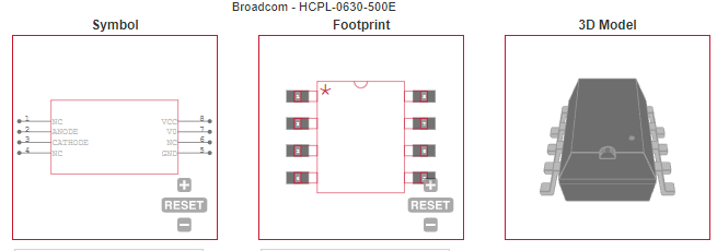
HCPL-0630-500E ECAD MODELS
|
HCPL-0630-500E APPLICATIONS
|
|
PARAMETRIC INFO
|
| Input Type |
DC |
| Output Type |
Open Collector |
| Polarity |
Inverting |
| Direction Type |
Uni-Directional |
| Standard |
CSA|UL |
| Logic Gate Type |
Inverter |
| Number of Channels per Chip |
2 |
| Maximum Data Rate |
10MBd(Typ) |
| Minimum Forward Voltage (V) |
1.4 |
| Maximum Working Insulation Voltage (V) |
567 |
| Maximum Propagation Delay Time (tPLH) (ns) |
75 |
| Maximum Propagation Delay Time (tPHL) (ns) |
75 |
| Common Mode Voltage (V) |
1000 |
| Minimum Common Mode Rejection (kV/us) |
5 |
| Maximum Pulse Width Distortion (ns) |
35 |
| Maximum Propagation Delay Skew (ns) |
40 |
| Typical Forward Voltage (V) |
1.5 |
| Maximum Forward Voltage (V) |
1.75 |
| Maximum Forward Current (mA) |
15 |
| Maximum Reverse Voltage (V) |
5 |
| Maximum Continuous Output Current (mA) |
50 |
| Maximum Power Dissipation (mW) |
60 |
| Minimum Isolation Voltage (Vrms) |
3750 |
| Typical Rise Time (us) |
0.024 |
| Typical Fall Time (us) |
0.01 |
| Maximum Propagation Delay Time (ns) |
75 |
| Minimum Operating Temperature (°C) |
-40 |
| Maximum Operating Temperature (°C) |
85 |
| Supplier Temperature Grade |
Industrial |
| Minimum Supply Voltage (V) |
4.5 |
| Maximum Supply Voltage (V) |
5.5 |
| Minimum Storage Temperature (°C) |
-55 |
| Maximum Storage Temperature (°C) |
125 |
|
|
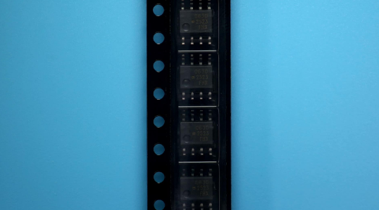
PACKAGE INFO
|
| Supplier Package |
SOIC |
| Basic Package Type |
Lead-Frame SMT |
| Pin Count |
8 |
| Lead Shape |
Gull-wing |
| PCB |
8 |
| Tab |
N/R |
| Pin Pitch (mm) |
1.27 |
| Package Length (mm) |
5.08 |
| Package Width (mm) |
3.94 |
| Package Height (mm) |
3.18 |
| Package Diameter (mm) |
N/R |
| Seated Plane Height (mm) |
3.38 |
| Mounting |
Surface Mount |
| Terminal Width (mm) |
0.41 |
| Package Weight (g) |
N/A |
| Package Material |
Plastic |
| Package Description |
Small Outline IC |
| Package Family Name |
SO |
| Jedec |
N/A |
| Package Outline |
Link to Datasheet |
|
|
MANUFACTURING INFO
|
| MSL |
1 |
| Maximum Reflow Temperature (°C) |
250 |
| Reflow Solder Time (Sec) |
30 |
| Number of Reflow Cycle |
3 |
| Standard |
J-STD-020E |
| Reflow Temp. Source |
Link to Datasheet |
| Maximum Wave Temperature (°C) |
N/R |
| Wave Solder Time (Sec) |
N/R |
| Lead Finish(Plating) |
Matte Sn annealed |
| Under Plating Material |
N/A |
| Terminal Base Material |
N/A |
| Number of Wave Cycles |
N/R |
|
|
PACKAGING INFO
|
| Packaging |
Tape and Reel |
| Quantity Of Packaging |
1500 |
| Packaging Document |
Link to Datasheet |
|
|
ECAD MODELS
|
|
|
| APPLICATIONS |
| • Isolated line receiver |
| • Computer-peripheral interfaces |
| • Microprocessor system interfaces |
| • Digital isolation for A/D, D/A conversion |
| • Switching power supply |
| • Instrument input/output isolation |
| • Ground loop elimination |
| • Pulse transformer replacement |
| • Power transistor isolation in motor drives |
| • Isolation of high speed logic systems |
| |