|
|
• Excellent DC Performance:
– Low Input Offset Voltage: 55 μV (max)
– Low Input Offset Drift: 0.2 μV/°C (max)
– High CMRR: 104 dB, G ≥ 10 (min)
|
• Low Input Noise:
– 12 nV/√Hz at 1 kHz
– 0.25 μVPP (0.1 Hz to 10 Hz)
|
• Wide Supply Range:
– Single Supply: 4 V to 36 V
– Dual Supply: ±2 V to ±18 V
|
• Gain Set with a Single External Resistor:
– Gain Equation: G = 1 + (50 kΩ / RG)
– Gain Error: 0.007%, G = 1
– Gain Drift: 5 ppm/°C (max) G = 1
|
• Input Voltage: (V–) + 0.1 V to (V+) – 1.5 V
|
• RFI-Filtered Inputs
|
• Rail-to-Rail Output
|
• Low Quiescent Current: 1.4 mA
|
• Operating Temperature: –55°C to +150°C
|
• SOIC-8 and DFN-8 Packages
|
|
| CATALOG |
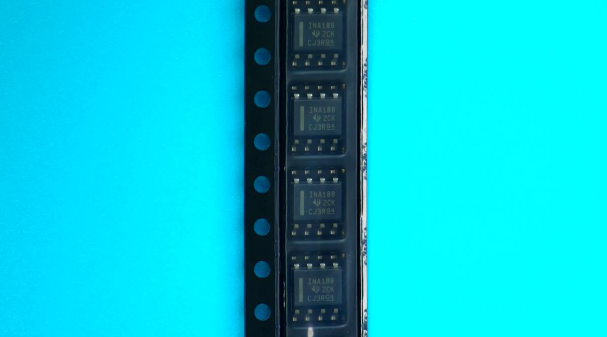
INA188IDR COUNTRY OF ORIGIN
|
INA188IDR PARAMETRIC INFO
|
INA188IDR PACKAGE INFO
|
INA188IDR MANUFACTURING INFO
|
INA188IDR PACKAGING INFO
|
INA188IDR APPLICATIONS
|
|
COUNTRY OF ORIGIN
|
Malaysia
|
|
PARAMETRIC INFO
|
| Rail to Rail |
Rail to Rail Output |
| Number of Channels per Chip |
1 |
| Minimum PSRR (dB) |
130.46(Typ) |
| Maximum Input Offset Voltage (mV) |
0.055@36V |
| Maximum Input Bias Current (uA) |
0.0025@36V |
| Minimum CMRR (dB) |
84 |
| Maximum Quiescent Current (mA) |
1.6@36V |
| Minimum CMRR Range (dB) |
80 to 85 |
| Minimum Single Supply Voltage (V) |
4 |
| Maximum Single Supply Voltage (V) |
36 |
| Minimum Dual Supply Voltage (V) |
±2 |
| Maximum Input Resistance (MOhm) |
0.04(Typ)@36V |
| Maximum Dual Supply Voltage (V) |
±18 |
| Maximum Voltage Gain Range (dB) |
60 to 75 |
| Maximum Voltage Gain (dB) |
60 |
| Minimum Operating Temperature (°C) |
-40 |
| Maximum Operating Temperature (°C) |
125 |
| Minimum Storage Temperature (°C) |
-65 |
| Maximum Storage Temperature (°C) |
150 |
| Power Supply Type |
Single|Dual |
| Maximum Supply Voltage Range (V) |
>=30 |
| Typical Single Supply Voltage (V) |
5|9|12|15|18|24|28 |
| Typical Dual Supply Voltage (V) |
±3|±5|±9|±12|±15 |
| Maximum Operating Supply Voltage (V) |
±18|36 |
|
|
PACKAGE INFO
|
| Supplier Package |
SOIC |
| Basic Package Type |
Lead-Frame SMT |
| Pin Count |
8 |
| Lead Shape |
Gull-wing |
| PCB |
8 |
| Tab |
N/R |
| Pin Pitch (mm) |
1.27 |
| Package Length (mm) |
5(Max) |
| Package Width (mm) |
3.98(Max) |
| Package Height (mm) |
1.5(Max) |
| Package Diameter (mm) |
N/R |
| Package Overall Length (mm) |
5(Max) |
| Package Overall Width (mm) |
6.19(Max) |
| Package Overall Height (mm) |
1.75(Max) |
| Seated Plane Height (mm) |
1.75(Max) |
| Mounting |
Surface Mount |
| Package Weight (g) |
N/A |
| Package Material |
Plastic |
| Package Description |
Small Outline IC |
| Package Family Name |
SO |
| Jedec |
MS-012AA |
| Package Outline |
Link to Datasheet |
|
|
MANUFACTURING INFO
|
| MSL |
2 |
| Maximum Reflow Temperature (°C) |
260 |
| Reflow Solder Time (Sec) |
30 |
| Number of Reflow Cycle |
3 |
| Standard |
J-STD-020D |
| Reflow Temp. Source |
Link to Datasheet |
| Maximum Wave Temperature (°C) |
N/R |
| Wave Solder Time (Sec) |
N/R |
| Lead Finish(Plating) |
Au |
| Under Plating Material |
Pd over Ni |
| Terminal Base Material |
Cu Alloy |
| Number of Wave Cycles |
N/R |
|
|
PACKAGING INFO
|
| Packaging Suffix |
R |
| Packaging |
Tape and Reel |
| Quantity Of Packaging |
2500 |
| Reel Diameter (in) |
13 |
| Reel Width (mm) |
12.4 |
| Tape Pitch (mm) |
8 |
| Tape Width (mm) |
12 |
| Component Orientation |
Q1 |
| Packaging Document |
Link to Datasheet |
|
|
APPLICATIONS
|
• Bridge Amplifiers
|
| • ECG Amplifiers |
| • Pressure Sensors |
| • Medical Instrumentation |
• Portable Instrumentation
|
• Weigh Scales
|
• Thermocouple Amplifiers
|
• RTD Sensor Amplifiers
|
• Data Acquisition
|
| |