|
|
• Input common-mode range: Includes V–
|
• Common-mode rejection:
– 104 dB, min (G = 10)
– 100 dB, min at 5 kHz (G = 10)
|
• Power-supply rejection: 100 dB, min (G = 1)
|
• Low offset voltage: 150 µV, max
|
• Gain drift: 1 ppm/°C (G = 1), 35 ppm/°C (G > 1)
|
• Noise: 18 nV/√Hz, G ≥ 100
|
• Bandwidth: 1 MHz (G = 1), 60 kHz (G = 100)
|
• Inputs protected up to ±40 V
|
• Rail-to-rail output
|
• Supply current: 200 µA
|
• Supply range:
– Single supply: 3 V to 36 V
– Dual supply: ±1.5 V to ±18 V
|
• Specified temperature range:
–40°C to +125°C
|
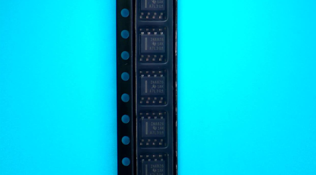
• Packages: 8-pin VSSOP, SOIC, and WSON
|
|
| CATALOG |
INA826AIDR COUNTRY OF ORIGIN
|
INA826AIDR PARAMETRIC INFO
|
INA826AIDR PACKAGE INFO
|
INA826AIDR MANUFACTURING INFO
|
INA826AIDR PACKAGING INFO
|
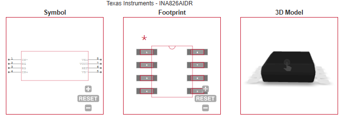
INA826AIDR ECAD MODELS
|
INA826AIDR APPLICATIONS
|
|
COUNTRY OF ORIGIN
|
Malaysia
|
|
PARAMETRIC INFO
|
| Rail to Rail |
Rail to Rail Output |
| Number of Channels per Chip |
1 |
| Minimum PSRR (dB) |
100 |
| Maximum Input Offset Voltage (mV) |
0.15@±15V |
| Maximum Input Bias Current (uA) |
0.065@±15V |
| Minimum CMRR (dB) |
84 |
| Maximum Quiescent Current (mA) |
0.25@±15V |
| Process Technology |
Bipolar |
| Minimum CMRR Range (dB) |
75 to 85 |
| Minimum Single Supply Voltage (V) |
3 |
| Maximum Single Supply Voltage (V) |
36 |
| Minimum Dual Supply Voltage (V) |
±1.5 |
| Maximum Input Resistance (MOhm) |
0.1(Typ)@±15V |
| Maximum Dual Supply Voltage (V) |
±18 |
| Maximum Voltage Gain Range (dB) |
60 to 75 |
| Maximum Voltage Gain (dB) |
60 |
| Minimum Operating Temperature (°C) |
-40 |
| Maximum Operating Temperature (°C) |
125 |
| Minimum Storage Temperature (°C) |
-65 |
| Maximum Storage Temperature (°C) |
150 |
| Power Supply Type |
Single|Dual |
| Maximum Supply Voltage Range (V) |
30 to 50 |
| Typical Single Supply Voltage (V) |
5|9|12|15|18|24|28 |
| Typical Dual Supply Voltage (V) |
±3|±5|±9|±12|±15 |
| Maximum Operating Supply Voltage (V) |
±18|36 |
|
|
PACKAGE INFO
|
| Supplier Package |
SOIC |
| Basic Package Type |
Lead-Frame SMT |
| Pin Count |
8 |
| Lead Shape |
Gull-wing |
| PCB |
8 |
| Tab |
N/R |
| Pin Pitch (mm) |
1.27 |
| Package Length (mm) |
5(Max) |
| Package Width (mm) |
3.98(Max) |
| Package Height (mm) |
1.5(Max) |
| Package Diameter (mm) |
N/R |
| Package Overall Length (mm) |
5(Max) |
| Package Overall Width (mm) |
6.19(Max) |
| Package Overall Height (mm) |
1.75(Max) |
| Seated Plane Height (mm) |
1.75(Max) |
| Mounting |
Surface Mount |
| Package Weight (g) |
N/A |
| Package Material |
Plastic |
| Package Description |
Small Outline IC |
| Package Family Name |
SO |
| Jedec |
MS-012AA |
| Package Outline |
Link to Datasheet |
|
|
MANUFACTURING INFO
|
| MSL |
2 |
| Maximum Reflow Temperature (°C) |
260 |
| Reflow Solder Time (Sec) |
30 |
| Number of Reflow Cycle |
3 |
| Standard |
J-STD-020D |
| Reflow Temp. Source |
Link to Datasheet |
| Maximum Wave Temperature (°C) |
N/R |
| Wave Solder Time (Sec) |
N/R |
| Lead Finish(Plating) |
Au |
| Under Plating Material |
Pd over Ni |
| Terminal Base Material |
Cu Alloy |
|
|
PACKAGING INFO
|
| Packaging Suffix |
R |
| Packaging |
Tape and Reel |
| Quantity Of Packaging |
2500 |
| Reel Diameter (in) |
13 |
| Reel Width (mm) |
12.4 |
| Tape Pitch (mm) |
8 |
| Tape Width (mm) |
12 |
| Component Orientation |
Q1 |
| Packaging Document |
Link to Datasheet |
|
|
ECAD MODELS
|
|
|
APPLICATIONS
|
• Analog input module
|
| • Flow transmitter |
• Battery test
|
• LCD test
|
| • Electrocardiogram (ECG)
|
| • Surgical equipment |
• Process analytics (pH, gas, concentration, force
and humidity)
|
• Circuit breaker (ACB, MCCB, VCB)
|
| |
| |