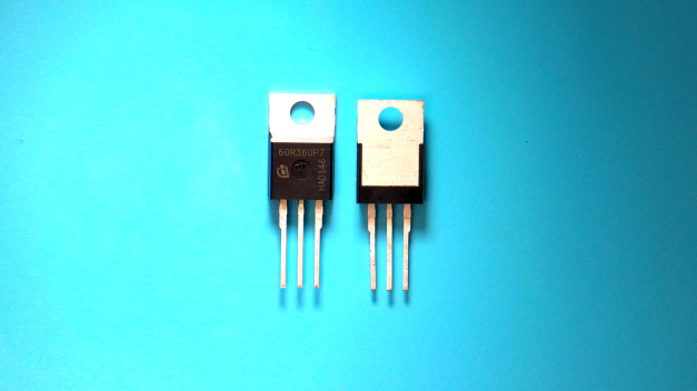
IPP60R360P7XKSA1 Infineon Technologies MOSFET N-CH 650V 9A TO220-3

label:
2024/05/6 289


• Suitableforhardandsoftswitching(PFCandLLC)duetoanoutstanding commutationruggedness
• Significantreductionofswitchingandconductionlosses
• ExcellentESDrobustness>2kV(HBM)forallproducts
• BetterRDS(on)/packageproductscomparedtocompetitionenabledbya lowRDS(on)*A(below1Oh
• Fullyqualifiedacc.JEDECforIndustrialApplications


CATALOG
IPP60R360P7XKSA1 COUNTRY OF ORIGIN
IPP60R360P7XKSA1 PARAMETRIC INFO
IPP60R360P7XKSA1 PACKAGE INFO
IPP60R360P7XKSA1 PACKAGING INFO


COUNTRY OF ORIGIN
Malaysia
China


PARAMETRIC INFO
Channel Type N
Channel Mode Enhancement
Configuration Single
Maximum Drain Source Voltage (V) 600
Maximum Continuous Drain Current (A) 9
Maximum Gate Source Voltage (V) 20
Maximum Drain Source Resistance (mOhm) 360@10V
Typical Gate Charge @ Vgs (nC) 13@10V
Typical Gate Charge @ 10V (nC) 13
Maximum Power Dissipation (mW) 41000
Process Technology CoolMOS P7
Category Power MOSFET
Typical Gate to Drain Charge (nC) 4
Maximum Junction Ambient Thermal Resistance 62K/W
Typical Input Capacitance @ Vds (pF) 555@400V
Typical Turn-On Delay Time (ns) 8
Typical Turn-Off Delay Time (ns) 42
Typical Fall Time (ns) 10
Typical Rise Time (ns) 7
Maximum Gate Source Leakage Current (nA) 1000
Maximum Gate Threshold Voltage (V) 4
Maximum IDSS (uA) 1
Number of Elements per Chip 1
Minimum Storage Temperature (°C) -55
Maximum Storage Temperature (°C) 150
Minimum Operating Temperature (°C) -55
Maximum Operating Temperature (°C) 150


PACKAGE INFO
Supplier Package TO-220
Pin Count 3
PCB 3
Tab Tab
Pin Pitch (mm) 2.54
Package Length (mm) 10.36(Max)
Package Width (mm) 4.57(Max)
Package Height (mm) 9.45(Max)
Package Diameter (mm) N/R
Mounting Through Hole
Package Material Plastic
Package Description Transistor Outline Package
Package Family Name TO
Package Outline Link to Datasheet


MANUFACTURING INFO
MSL 2
Maximum Reflow Temperature (°C) 260
Reflow Solder Time (Sec) 30
Number of Reflow Cycle 3
Standard J-STD-020D
Reflow Temp. Source Link to Datasheet
Maximum Wave Temperature (°C) N/R
Wave Solder Time (Sec) N/R
Lead Finish(Plating) Au
Under Plating Material Pd over Ni
Terminal Base Material Cu Alloy
Shelf Life Period 2 Years
Number of Wave Cycles N/R


PACKAGING INFO
Packaging Tube
Quantity Of Packaging 500

Продукт RFQ