|
| |
• Floating channel designed for bootstrap operation
|
• Fully operational to +1200 V
|
• Tolerant to negative transient voltage
|
| • dV/dt immune |
| • Gate drive supply range from 12 V to 20 V |
| • Undervoltage lockout for both channels |
| • 3.3 V logic compatible |
| • Separate logic supply range from 3.3 V to 20 V |
| • Logic and power ground ±5 V offset |
| • CMOS Schmitt-triggered inputs with pull-down |
| • Cycle by cycle edge-triggered shutdown logic |
| • Matched propagation delay for both channels |
| • Outputs in phase with inputs |
| |
| CATALOG |
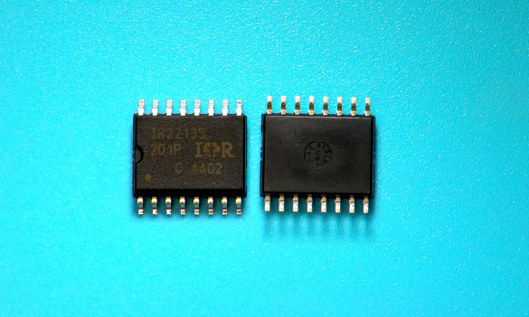
| IR2213SPBF COUNTRY OF ORIGIN |
IR2213SPBF PARAMETRIC INFO
|
IR2213SPBF PACKAGE INFO
|
IR2213SPBF MANUFACTURING INFO
|
IR2213SPBF PACKAGING INFO
|
|
| COUNTRY OF ORIGIN |
| Malaysia |
| Thailand |
| United States of America |
|
PARAMETRIC INFO
|
| Driver Type |
High and Low Side |
| Number of Drivers |
2 |
| Bridge Type |
Half Bridge |
| Input Logic Compatibility |
CMOS|LSTTL|3.3V(Min) |
| Maximum Operating Supply Voltage (V) |
20 |
| Type |
IGBT|MOSFET |
| Maximum Operating Temperature (°C) |
125 |
| Maximum Turn-Off Delay Time (ns) |
30 |
| Maximum Turn-On Delay Time (ns) |
30 |
| High and Low Sides Dependency |
Independent |
| Number of Outputs |
2 |
| Maximum Power Dissipation (mW) |
1000 |
| Minimum Operating Supply Voltage (V) |
12 |
| Absolute Propagation Delay Time (ns) |
280(Typ) |
| Maximum Propagation Delay Time (ns) |
280(Typ) |
| Maximum Rise Time (ns) |
25(Typ) |
| Maximum Fall Time (ns) |
17(Typ) |
| Typical Input High Threshold Voltage (V) |
9.5(Min) |
| Typical Input Low Threshold Voltage (V) |
6(Max) |
| Latch-Up Proof |
No |
| Special Features |
Undervoltage Lockout|Matched Propagation Delay |
| Minimum Storage Temperature (°C) |
-55 |
| Maximum Storage Temperature (°C) |
150 |
|
|
PACKAGE INFO
|
| Supplier Package |
SOIC W |
| Basic Package Type |
Lead-Frame SMT |
| Pin Count |
16 |
| Lead Shape |
Gull-wing |
| PCB |
16 |
| Tab |
N/R |
| Pin Pitch (mm) |
1.27 |
| Package Length (mm) |
10.5(Max) |
| Package Width (mm) |
7.6(Max) |
| Package Height (mm) |
2.35(Max) |
| Package Diameter (mm) |
N/R |
| Seated Plane Height (mm) |
2.65(Max) |
| Mounting |
Surface Mount |
| Package Material |
Plastic |
| Package Description |
Small Outline IC Wide Body |
| Package Family Name |
SO |
| Jedec |
MS-013AA |
| Package Outline |
Link to Datasheet |
|
|
MANUFACTURING INFO
|
| MSL |
3 |
| Maximum Reflow Temperature (°C) |
260 |
| Reflow Solder Time (Sec) |
10 to 30 |
| Reflow Temp. Source |
Link to Datasheet |
| Maximum Wave Temperature (°C) |
300 |
| Wave Solder Time (Sec) |
10 |
| Wave Temp. Source |
Link to Datasheet |
| Lead Finish(Plating) |
Matte Sn annealed |
| Under Plating Material |
N/A |
| Terminal Base Material |
Cu Alloy |
| Shelf Life Period |
3 Years |
|
|
PACKAGING INFO
|
| Packaging |
Tube |
| Quantity Of Packaging |
1980 |
|
| |