|
|
• Key Parameters Optimized for Class-D Audio
Amplifier Applications
|
• Low RDSON for Improved Efficiency
|
• Low QG and QSW for Better THD and Improved
Efficiency
|
• Low QRR for Better THD and Lower EMI
|
• 175°C Operating Junction Temperature for
Ruggedness
|
• Can Deliver up to 200W per Channel into 8Ω Load in
Half-Bridge Configuration Amplifier
|
|
| CATALOG |
| IRFB4019PBF COUNTRY OF ORIGIN |
IRFB4019PBF PARAMETRIC INFO
|
IRFB4019PBF PACKAGE INFO
|
IRFB4019PBF MANUFACTURING INFO
|
IRFB4019PBF PACKAGING INFO
|
|
COUNTRY OF ORIGIN
|
China
|
Malaysia
|
Philippines
|
Taiwan (Province of China)
|
United States of America
|
Israel
|
Korea (Republic of)
|
Mexico
|
United Kingdom of Great Britain and Northern Ireland
|
|
PARAMETRIC INFO
|
| Channel Type |
N |
| Channel Mode |
Enhancement |
| Configuration |
Single |
| Maximum Drain Source Voltage (V) |
150 |
| Material |
Si |
| Maximum Continuous Drain Current (A) |
17 |
| Maximum Gate Source Voltage (V) |
±20 |
| Maximum Drain Source Resistance (mOhm) |
95@10V |
| Typical Gate Charge @ Vgs (nC) |
13@10V |
| Typical Gate Charge @ 10V (nC) |
13 |
| Maximum Power Dissipation (mW) |
80000 |
| Category |
Power MOSFET |
| Typical Input Capacitance @ Vds (pF) |
800@50V |
| Typical Turn-On Delay Time (ns) |
7 |
| Typical Turn-Off Delay Time (ns) |
12 |
| Typical Fall Time (ns) |
7.8 |
| Typical Rise Time (ns) |
13 |
| Number of Elements per Chip |
1 |
| Minimum Operating Temperature (°C) |
-55 |
| Maximum Operating Temperature (°C) |
175 |
|
|
PACKAGE INFO
|
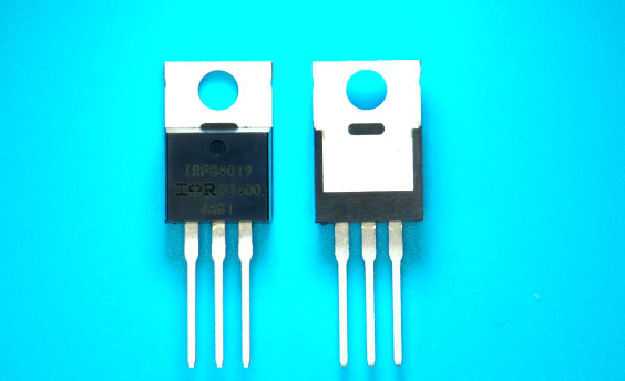
| Supplier Package |
TO-220AB |
| Basic Package Type |
Through Hole |
| Pin Count |
3 |
| Lead Shape |
Through Hole |
| PCB |
3 |
| Tab |
Tab |
| Pin Pitch (mm) |
2.54 |
| Package Length (mm) |
10.66(Max) |
| Package Width (mm) |
4.82(Max) |
| Package Height (mm) |
9.02(Max) |
| Package Diameter (mm) |
N/R |
| Seated Plane Height (mm) |
19.83(Max) |
| Mounting |
Through Hole |
| Package Material |
Plastic |
| Package Description |
Transistor Outline Package |
| Package Family Name |
TO-220 |
| Jedec |
TO-220AB |
| Package Outline |
Link to Datasheet |
|
|
MANUFACTURING INFO
|
| MSL |
N/R |
| Maximum Reflow Temperature (°C) |
260 |
| Reflow Solder Time (Sec) |
N/A |
| Number of Reflow Cycle |
N/A |
| Reflow Temp. Source |
Link to Datasheet |
| Maximum Wave Temperature (°C) |
300 |
| Wave Solder Time (Sec) |
N/A |
| Wave Temp. Source |
Link to Datasheet |
| Lead Finish(Plating) |
Matte Sn annealed |
| Under Plating Material |
Ni |
| Terminal Base Material |
Cu Alloy |
| Shelf Life Period |
3 Years |
| Number of Wave Cycles |
N/A |
|
|
PACKAGING INFO
|
| Packaging |
Tube |
| Quantity Of Packaging |
1000 |
|
|