 |
|
| CATALOG |
| IRFS7440TRLPBF COUNTRY OF ORIGIN |
| IRFS7440TRLPBF PARAMETRIC INFO |
| IRFS7440TRLPBF PACKAGE INFO |
| IRFS7440TRLPBF MANUFACTURING INFO |
| IRFS7440TRLPBF PACKAGING INFO |
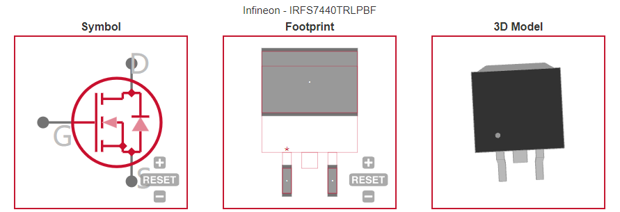
| IRFS7440TRLPBF ECAD MODELS |
| IRFS7440TRLPBF APPLICATIONS |
|
| COUNTRY OF ORIGIN |
| China |
| Israel |
| Mexico |
| Taiwan (Province of China) |
| United Kingdom of Great Britain and Northern Ireland |
|
| PARAMETRIC INFO |
| Channel Type |
N |
| Channel Mode |
Enhancement |
| Configuration |
Single |
| Maximum Drain Source Voltage (V) |
40 |
| Maximum Continuous Drain Current (A) |
208 |
| Maximum Gate Source Voltage (V) |
±20 |
| Maximum Drain Source Resistance (mOhm) |
2.5@10V |
| Typical Gate Charge @ Vgs (nC) |
90@10V |
| Typical Gate Charge @ 10V (nC) |
90 |
| Maximum Power Dissipation (mW) |
208000 |
| Process Technology |
HEXFET |
| Category |
Power MOSFET |
| Typical Input Capacitance @ Vds (pF) |
4730@25V |
| Typical Turn-On Delay Time (ns) |
24 |
| Typical Turn-Off Delay Time (ns) |
115 |
| Typical Fall Time (ns) |
68 |
| Typical Rise Time (ns) |
68 |
| Maximum Gate Source Leakage Current (nA) |
100 |
| Maximum Gate Threshold Voltage (V) |
3.9 |
| Maximum IDSS (uA) |
1 |
| Number of Elements per Chip |
1 |
| Minimum Storage Temperature (°C) |
-55 |
| Maximum Storage Temperature (°C) |
175 |
| Minimum Operating Temperature (°C) |
-55 |
| Maximum Operating Temperature (°C) |
175 |
|
| PACKAGE INFO |
| Supplier Package |
D2PAK |
| Basic Package Type |
Lead-Frame SMT |
| Pin Count |
3 |
| Lead Shape |
Gull-wing |
| PCB |
2 |
| Tab |
Tab |
| Pin Pitch (mm) |
2.54 |
| Package Length (mm) |
10.67(Max) |
| Package Width (mm) |
9.65(Max) |
| Package Height (mm) |
4.83(Max) |
| Package Diameter (mm) |
N/R |
| Package Overall Length (mm) |
10.67(Max) |
| Package Overall Width (mm) |
15.88(Max) |
| Package Overall Height (mm) |
5.08(Max) |
| Seated Plane Height (mm) |
5.08(Max) |
| Mounting |
Surface Mount |
| Package Material |
Plastic |
| Package Description |
Double Deca Watt Package |
| Package Family Name |
TO-263 |
| Jedec |
TO-263AB |
| Package Outline |
Link to Datasheet |
|
| MANUFACTURING INFO |
| MSL |
1 |
| Maximum Reflow Temperature (°C) |
245 |
| Reflow Solder Time (Sec) |
30 |
| Number of Reflow Cycle |
3 |
| Standard |
J-STD-020D |
| Reflow Temp. Source |
Link to Datasheet |
| Maximum Wave Temperature (°C) |
300 |
| Wave Solder Time (Sec) |
10 |
| Wave Temp. Source |
Link to Datasheet |
| Lead Finish(Plating) |
Matte Sn |
| Under Plating Material |
N/A|Ni |
| Terminal Base Material |
Cu |
| Shelf Life Period |
3 Years |
|
| PACKAGING INFO |
| Packaging Suffix |
TR |
| Packaging |
Tape and Reel |
| Quantity Of Packaging |
800 |
| Packaging Document |
Link to Datasheet |
|
| ECAD MODELS |
 |
|
| APPLICATIONS |
| • Brushed Motor drive applications
|
| • BLDC Motor drive applications |
| • Battery powered circuits
|
| • Half-bridge and full-bridge topologies |
| • Synchronous rectifier applications
|
| • Resonant mode power supplies |
| • OR-ing and redundant power switches |
| • DC/DC and AC/DC converters |
| • DC/AC Inverters |
|