 |
|
| • Isolated bidirectional, I2C compatible,
communication |
| • Supports up to 1-MHz operation |
| • 3-V to 5.5-V supply range |
| • Open-drain outputs With 3.5-mA Side 1 and 35-
mA Side 2 sink current capability |
| • –40°C to +125°C operating temperature |
| • ±50-kV/µs transient immunity (Typical) |
| • HBM ESD protection of 4 kV on all pins;
8 kV on bus pins |
• Safety-related certifications:
– 4242-VPK isolation per DIN EN IEC 60747-17(VDE 0884-17)
– 2500-VRMS isolation for 1 minute per UL 1577
– CSA approval per IEC 62368-1 end equipmentstandard
– CQC basic insulation per GB4943.1-2011 |
|
| CATALOG |
| ISO1541DR COUNTRY OF ORIGIN |
| ISO1541DR PARAMETRIC INFO |
| ISO1541DR PACKAGE INFO |
| ISO1541DR MANUFACTURING INFO |
| ISO1541DR PACKAGING INFO |
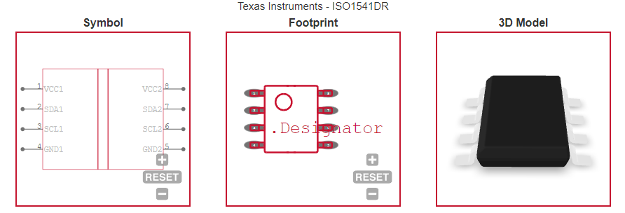
| ISO1541DR ECAD MODELS |
| ISO1541DR FUNCTIONAL BLOCK DIAGRAMS |
| ISO1541DR APPLICATIONS
|
|
| COUNTRY OF ORIGIN |
| Taiwan (Province of China) |
| Malaysia |
|
| PARAMETRIC INFO |
| Number of Channels per Chip |
2 |
| Type |
I2C |
| Isolated Power |
No |
| Output Type |
Open Drain |
| Minimum Isolation Voltage (Vrms) |
2500 |
| Maximum Power Dissipation (mW) |
105 |
| Maximum Pulse Width Distortion (ns) |
123 |
| Minimum Common Mode Rejection (kV/us) |
25 |
| Maximum Working Insulation Voltage |
566Vp |
| Maximum Fall Time (ns) |
100 |
| Maximum Propagation Delay Time (tPHL) (ns) |
181 |
| Maximum Propagation Delay Time (tPLH) (ns) |
65 |
| Maximum Data Rate |
1Mbps |
| Minimum Operating Supply Voltage (V) |
3 |
| Typical Operating Supply Voltage (V) |
3.3|5 |
| Maximum Operating Supply Voltage (V) |
5.5 |
| Minimum Operating Temperature (°C) |
-40 |
| Maximum Operating Temperature (°C) |
125 |
| Maximum Output Current Drive (mA) |
100 |
| Coupling Type |
Capacitive Coupling |
| Forward/Reverse Channels |
1/1 |
| Minimum Storage Temperature (°C) |
-65 |
| Maximum Storage Temperature (°C) |
150 |
|
| |
| PACKAGE INFO |
| Supplier Package |
SOIC |
| Basic Package Type |
Lead-Frame SMT |
| Pin Count |
8 |
| Lead Shape |
Gull-wing |
| PCB |
8 |
| Tab |
N/R |
| Pin Pitch (mm) |
1.27 |
| Package Length (mm) |
5(Max) |
| Package Width (mm) |
3.98(Max) |
| Package Height (mm) |
1.5(Max) |
| Package Diameter (mm) |
N/R |
| Package Overall Length (mm) |
5(Max) |
| Package Overall Width (mm) |
6.19(Max) |
| Package Overall Height (mm) |
1.75(Max) |
| Seated Plane Height (mm) |
1.75(Max) |
| Mounting |
Surface Mount |
| Package Weight (g) |
N/A |
| Package Material |
Plastic |
| Package Description |
Small Outline IC |
| Package Family Name |
SO |
| Jedec |
MS-012AA |
| Package Outline |
Link to Datasheet |
|
| |
| MANUFACTURING INFO |
| MSL |
2 |
| Maximum Reflow Temperature (°C) |
260 |
| Reflow Solder Time (Sec) |
30 |
| Number of Reflow Cycle |
3 |
| Standard |
J-STD-020D |
| Reflow Temp. Source |
Link to Datasheet |
| Maximum Wave Temperature (°C) |
260 |
| Wave Solder Time (Sec) |
5 |
| Lead Finish(Plating) |
Au |
| Under Plating Material |
Pd over Ni |
| Terminal Base Material |
Cu Alloy |
| Number of Wave Cycles |
3 |
|
| |
| PACKAGING INFO |
| Packaging Suffix |
R |
| Packaging |
Tape and Reel |
| Quantity Of Packaging |
2500 |
| Reel Diameter (in) |
13 |
| Reel Width (mm) |
12.4 |
| Tape Pitch (mm) |
8 |
| Tape Width (mm) |
12 |
| Component Orientation |
Q1 |
| Packaging Document |
Link to Datasheet |
|
| |
| ECAD MODELS |
 |
|
| FUNCTIONAL BLOCK DIAGRAMS |
 |
|
| APPLICATIONS
|
| • Isolated I2C buses |
| • SMBus and PMBus interfaces
|
| • Open-drain networks |
| • Motor control systems |
| • Battery management |
| • I
2C level shifting
|
| |
|