 |
|
| • Low dropout voltage (1 V typ.) |
| • 2.85 V device performances are suitable for
SCSI-2 active termination |
| • Output current up to 800 mA |
| • Fixed output voltage of: 1.2 V, 1.8 V, 2.5 V,
3.3 V, 5.0 V |
| • Adjustable version availability (VREF = 1.25 V) |
| • Internal current and thermal limit
|
| • Available in ± 1 % (at 25 °C) and 2 % in full
temperature range |
| • Supply voltage rejection: 75 dB (typ.) |
|
| CATALOG |
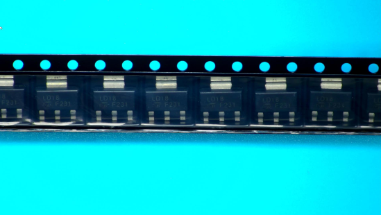
| LD1117S18CTR COUNTRY OF ORIGIN |
| LD1117S18CTR PARAMETRIC INFO |
| LD1117S18CTR PACKAGE INFO |
| LD1117S18CTR MANUFACTURING INFO |
| LD1117S18CTR PACKAGING INFO |
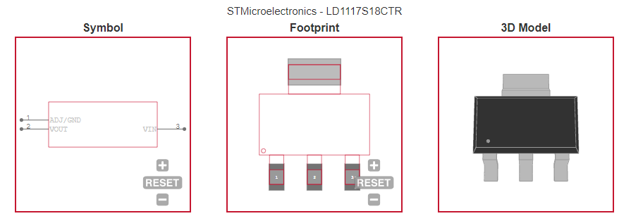
| LD1117S18CTR ECAD MODELS |
| LD1117S18CTR FUNCTONAL BLOCK DIAGRAM |
|
| COUNTRY OF ORIGIN |
| China |
| Israel |
| Malaysia |
| Singapore |
| United States of America |
|
| PARAMETRIC INFO |
| Type |
LDO |
| Number of Outputs |
1 |
| Maximum Output Current (A) |
1.3 |
| Minimum Operating Temperature (°C) |
-40 |
| Maximum Operating Temperature (°C) |
125 |
| Output Type |
Fixed |
| Output Voltage Range (V) |
1.8 to 10 |
| Junction to Ambient |
110°C/W |
| Junction to Case |
15°C/W |
| Polarity |
Positive |
| Special Features |
Current Limit|Thermal Protection |
| Load Regulation |
10mV |
| Line Regulation |
30mV |
| Maximum Quiescent Current (mA) |
10 |
| Maximum Dropout Voltage @ Current (V) |
1.1@100mA|1.15@500mA|1.2@800mA |
| Maximum Power Dissipation (mW) |
12000 |
| Maximum Input Voltage (V) |
15 |
| Output Voltage (V) |
1.8 |
| Typical Quiescent Current (mA) |
5 |
| Typical Dropout Voltage @ Current (V) |
1@100mA|1.05@500mA|1.1@800mA |
| Accuracy (%) |
±1 |
| Minimum Storage Temperature (°C) |
-40 |
| Maximum Storage Temperature (°C) |
150 |
| Typical PSRR (dB) |
75 |
| Typical Output Capacitance (uF) |
10(Min) |
| Typical Output Noise Voltage (uVrms) |
100 |
|
| PACKAGE INFO |
| Supplier Package |
SOT-223 |
| Basic Package Type |
Lead-Frame SMT |
| Pin Count |
4 |
| Lead Shape |
Gull-wing |
| PCB |
3 |
| Tab |
Tab |
| Pin Pitch (mm) |
2.3 |
| Package Length (mm) |
6.5 |
| Package Width (mm) |
3.5 |
| Package Height (mm) |
1.8(Max) |
| Package Diameter (mm) |
N/R |
| Seated Plane Height (mm) |
1.9(Max) |
| Mounting |
Surface Mount |
| Package Weight (g) |
N/A |
| Package Material |
Plastic |
| Package Description |
Small Outline Transistor |
| Package Family Name |
SOT |
| Jedec |
TO-261AA |
| Package Outline |
Link to Datasheet |
|
| MANUFACTURING INFO |
| MSL |
1 |
| Maximum Reflow Temperature (°C) |
260 |
| Reflow Solder Time (Sec) |
30 |
| Number of Reflow Cycle |
3 |
| Standard |
N/A |
| Reflow Temp. Source |
Link to Datasheet |
| Maximum Wave Temperature (°C) |
N/R |
| Wave Solder Time (Sec) |
N/R |
| Lead Finish(Plating) |
Matte Sn |
| Under Plating Material |
N/A |
| Terminal Base Material |
Cu Alloy |
| Shelf Life Period |
2 Years |
| Number of Wave Cycles |
N/R |
|
| PACKAGING INFO |
| Packaging Suffix |
TR |
| Packaging |
Tape and Reel |
| Quantity Of Packaging |
1000 |
| Packaging Document |
Link to Datasheet |
|
| ECAD MODELS |
 |
|
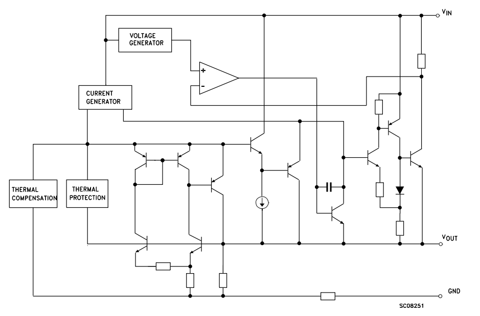
| FUNCTONAL BLOCK DIAGRAM |
 |
|