|
|
• 1.5 A guaranteed output current
|
• Ultra low dropout voltage (200 mV typ. @ 1.5 A load, 40 mV typ. @ 300 mA load)
|
• Very low quiescent current (1 mA typ. @ 1.5 A load, 1 µA max @ 25 °C in off mode)
|
• Logic-controlled electronic shutdown
|
• Current and thermal internal limit
|
• 1.5% output voltage tolerance @ 25 °C
|
• Fixed and ADJ output voltages: 1.8 V, 2.5 V, 3.3 V, ADJ
|
|
| CATALOG |
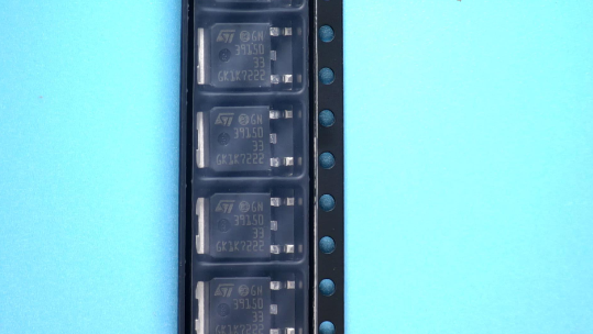
LD39150DT33-R COUNTRY OF ORIGIN
|
LD39150DT33-R PARAMETRIC INFO
|
LD39150DT33-R PACKAGE INFO
|
LD39150DT33-R MANUFACTURING INFO
|
LD39150DT33-R PACKAGING INFO
|
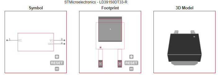
LD39150DT33-R ECAD MODELS
|
LD39150DT33-R APPLICATIONS
|
|
COUNTRY OF ORIGIN
|
China
|
|
PARAMETRIC INFO
|
| Type |
LDO |
| Number of Outputs |
1 |
| Maximum Output Current (A) |
1.5 |
| Minimum Operating Temperature (°C) |
-40 |
| Maximum Operating Temperature (°C) |
125 |
| Output Type |
Fixed |
| Output Voltage Range (V) |
1.8 to 10 |
| Junction to Ambient |
100°C/W |
| Junction to Case |
8°C/W |
| Polarity |
Positive |
| Special Features |
Current Limit|Thermal Shutdown Protection |
| Load Regulation |
0.06%/A(Typ) |
| Line Regulation |
0.04%(Typ) |
| Maximum Quiescent Current (mA) |
2.5 |
| Maximum Dropout Voltage @ Current (V) |
0.08@300mA|0.4@1500mA |
| Minimum Input Voltage (V) |
2.5 |
| Maximum Input Voltage (V) |
6 |
| Output Voltage (V) |
3.3 |
| Typical Quiescent Current (mA) |
1 |
| Typical Dropout Voltage @ Current (V) |
0.04@300mA|0.2@1500mA |
| Reference Voltage (V) |
1.22(Typ) |
| Accuracy (%) |
±1.5 |
| Minimum Storage Temperature (°C) |
-50 |
| Maximum Storage Temperature (°C) |
150 |
|
|
PACKAGE INFO
|
| Supplier Package |
DPAK |
| Pin Count |
3 |
| Lead Shape |
Gull-wing |
| PCB |
2 |
| Tab |
Tab |
| Pin Pitch (mm) |
2.3(Max) |
| Package Length (mm) |
6.6(Max) |
| Package Width (mm) |
6.2(Max) |
| Package Height (mm) |
2.4(Max) |
| Package Diameter (mm) |
N/R |
| Package Overall Length (mm) |
6.6(Max) |
| Package Overall Width (mm) |
10.1(Max) |
| Package Overall Height (mm) |
2.63(Max) |
| Seated Plane Height (mm) |
2.63(Max) |
| Mounting |
Surface Mount |
| Package Material |
Plastic |
| Package Description |
Deca Watt Package |
| Package Family Name |
TO-252 |
| Jedec |
TO-252AA |
| Package Outline |
Link to Datasheet |
|
|
MANUFACTURING INFO
|
| MSL |
1 |
| Maximum Reflow Temperature (°C) |
260 |
| Reflow Solder Time (Sec) |
30 |
| Number of Reflow Cycle |
3 |
| Reflow Temp. Source |
Link to Datasheet |
| Maximum Wave Temperature (°C) |
N/R |
| Wave Solder Time (Sec) |
N/R |
| Wave Temp. Source |
Link to Datasheet |
| Lead Finish(Plating) |
Matte Sn annealed |
| Under Plating Material |
N/A |
| Terminal Base Material |
Cu Alloy |
| Shelf Life Period |
2 Years |
|
|
PACKAGING INFO
|
| Packaging Suffix |
R |
| Packaging |
Tape and Reel |
| Packaging Document |
Link to Datasheet |
|
|
ECAD MODELS
|
 |
|
| APPLICATIONS |
| • Microprocessor power supply |
| • DSPs power supply |
| • Post regulators for switching suppliers |
| • High efficiency linear regulator |
| |