 |
|
| • For a newer drop-in alternative, see the TLV1117 |
| • For drop-in replacements in fixed output SOT-223
package configuration and improved functionality,
see the TLV761 |
| • Available in 1.8 V, 2.5 V, 3.3 V, 5 V, and adjustable
versions |
| • Space-saving SOT-223 and WSON packages |
| • Current limiting and thermal protection
|
| • Output current: 800 mA |
| • Line regulation: 0.2% (maximum) |
| • Load regulation: 0.4% (maximum) |
• Temperature range:
– LM1117: 0°C to +125°C
– LM1117I: –40°C to +125°C |
|
| CATALOG |
| LM1117MPX-3.3/NOPB COUNTRY OF ORIGIN |
| LM1117MPX-3.3/NOPB PARAMETRIC INFO |
| LM1117MPX-3.3/NOPB PACKAGE INFO |
| LM1117MPX-3.3/NOPB MANUFACTURING INFO |
| LM1117MPX-3.3/NOPB PACKAGING INFO |
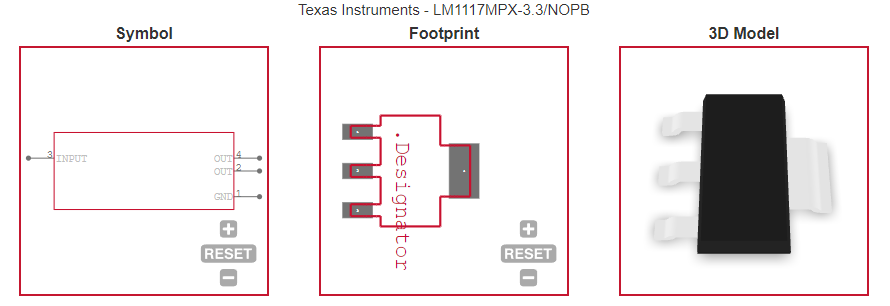
| LM1117MPX-3.3/NOPB ECAD MODELS |
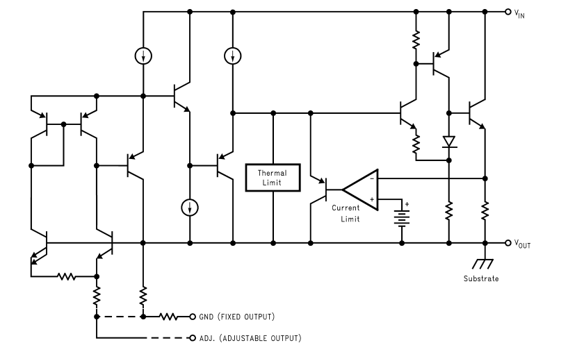
| LM1117MPX-3.3/NOPB FUNCTIONAL BLOCK DIAGRAM
|
| LM1117MPX-3.3/NOPB APPLICATIONS
|
|
| COUNTRY OF ORIGIN |
| China |
| Malaysia |
|
| PARAMETRIC INFO |
| Type |
LDO |
| Number of Outputs |
1 |
| Maximum Output Current (A) |
0.8 |
| Minimum Operating Temperature (°C) |
0 |
| Maximum Operating Temperature (°C) |
125 |
| Output Type |
Fixed |
| Output Voltage Range (V) |
1.8 to 10 |
| Junction to Ambient |
61.6°C/W |
| Junction to Case |
42.5°C/W |
| Polarity |
Positive |
| Special Features |
Current Limit|Thermal Protection |
| Load Regulation |
1mV(Typ) |
| Line Regulation |
1mV(Typ) |
| Maximum Quiescent Current (mA) |
10 |
| Maximum Dropout Voltage @ Current (V) |
1.2@100mA|1.25@500mA|1.3@800mA |
| Minimum Input Voltage (V) |
2.6 |
| Maximum Input Voltage (V) |
15 |
| Output Voltage (V) |
3.3 |
| Typical Quiescent Current (mA) |
5 |
| Typical Dropout Voltage @ Current (V) |
1.1@100mA|1.15@500mA|1.2@800mA |
| Accuracy (%) |
±1 |
| Minimum Storage Temperature (°C) |
-65 |
| Maximum Storage Temperature (°C) |
150 |
| Typical PSRR (dB) |
75 |
| Typical Output Capacitance (uF) |
10(Min) |
| Typical Output Noise Voltage (uVrms) |
38 |
| Output Capacitor Type |
Tantalum |
|
| |
| PACKAGE INFO |
| Supplier Package |
SOT-223 |
| Basic Package Type |
Lead-Frame SMT |
| Pin Count |
4 |
| Lead Shape |
Gull-wing |
| PCB |
3 |
| Tab |
Tab |
| Pin Pitch (mm) |
2.3 |
| Package Length (mm) |
6.7(Max) |
| Package Width (mm) |
3.7(Max) |
| Package Height (mm) |
1.7(Max) |
| Package Diameter (mm) |
N/R |
| Seated Plane Height (mm) |
1.8(Max) |
| Mounting |
Surface Mount |
| Package Weight (g) |
N/A |
| Package Material |
Plastic |
| Package Description |
Small Outline Transistor |
| Package Family Name |
SOT |
| Jedec |
TO-261AA |
| Package Outline |
Link to Datasheet |
|
| |
| MANUFACTURING INFO |
| MSL |
1 |
| Maximum Reflow Temperature (°C) |
260 |
| Reflow Solder Time (Sec) |
30 |
| Number of Reflow Cycle |
3 |
| Standard |
J-STD-020D |
| Reflow Temp. Source |
Link to Datasheet |
| Maximum Wave Temperature (°C) |
260 |
| Wave Solder Time (Sec) |
4 |
| Wave Temp. Source |
Link to Datasheet |
| Lead Finish(Plating) |
Matte Sn |
| Under Plating Material |
N/A |
| Terminal Base Material |
Cu Alloy |
| Number of Wave Cycles |
N/A |
|
| |
| PACKAGING INFO |
| Packaging Suffix |
X |
| Packaging |
Tape and Reel |
| Quantity Of Packaging |
2000 |
| Reel Diameter (in) |
13 |
| Reel Width (mm) |
16.4 |
| Tape Pitch (mm) |
12 |
| Tape Width (mm) |
16 |
| Component Orientation |
Q3 |
| Packaging Document |
Link to Datasheet |
|
| |
| ECAD MODELS |
 |
|
| FUNCTIONAL BLOCK DIAGRAM
|
 |
|
| APPLICATIONS |
| • AC drive power stage modules |
| • Merchant network and server PSU |
| • Industrial AC/DC |
| • Ultrasound scanners |
| • Servo drive control modules |
|