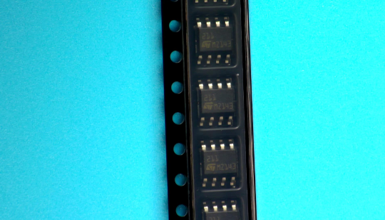
LM211DT STMicroelectronics IC VOLTAGE COMPARATOR 8-SOIC

label:
2023/11/7 308


• Maximum input current: 150 nA
• Maximum offset current: 20 nA  
• Differential input voltage range: ±30 V
• Power consumption:135 mW at ±15 V  
• Supply voltage: +5 V to ±15 V
• Output current: 50 mA  


CATALOG
LM211DT COUNTRY OF ORIGIN
LM211DT PARAMETRIC INFO
LM211DT PACKAGE INFO
LM211DT MANUFACTURING INFO
LM211DT PACKAGING INFO
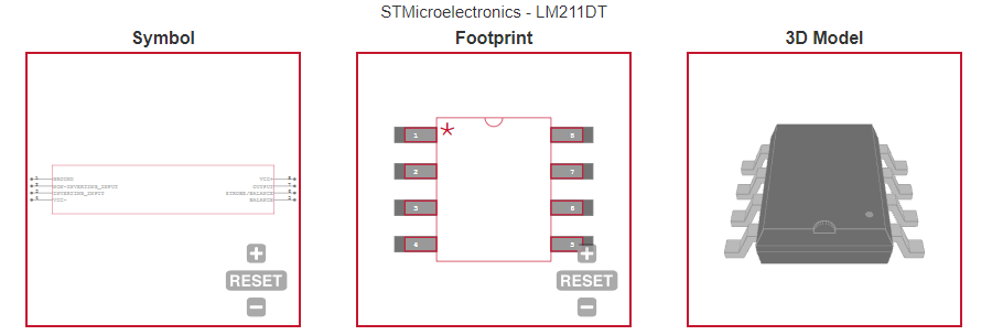
LM211DT ECAD MODELS


COUNTRY OF ORIGIN
China
Costa Rica
Malaysia
Morocco
Philippines
Thailand


PARAMETRIC INFO
Rail to Rail No
Manufacturer Type Voltage Comparator
Number of Channels per Chip 1
Output Type Open Collector
Maximum Input Offset Voltage (mV) 3@±15V
Maximum Input Bias Current (uA) 0.1@±15V
Maximum Input Voltage Range (V) ±15
Typical Voltage Gain (dB) 106.02
Typical Voltage Gain Range (dB) 90 to 110
Strobe Capability Yes
Typical Output Current (mA) 50
Typical Response Time (us) 0.2
Typical Response Time Range (us) 0.05 to 0.5
Minimum Operating Temperature (°C) -40
Maximum Operating Temperature (°C) 105
Minimum Storage Temperature (°C) -65
Maximum Storage Temperature (°C) 150
Power Supply Type Single|Dual
Integrated Voltage Reference No
Maximum Test Temperature (°C) 105
Minimum Test Temperature (°C) -40
Maximum Operating Supply Voltage (V) ±15|30
Integrated OP Amp No
Minimum Single Supply Voltage (V) 5
Typical Single Supply Voltage (V) 9|12|15|18|24|28
Maximum Single Supply Voltage (V) 30
Minimum Dual Supply Voltage (V) ±2.5
Typical Dual Supply Voltage (V) ±3|±5|±9|±12
Maximum Dual Supply Voltage (V) ±15
Maximum Supply Current (mA) 6@±15V
Maximum Power Dissipation (mW) 710
 
PACKAGE INFO
Supplier Package SO N
Basic Package Type Lead-Frame SMT
Pin Count 8
Lead Shape Gull-wing
PCB 8
Tab N/R
Pin Pitch (mm) 1.27
Package Length (mm) 5(Max)
Package Width (mm) 4(Max)
Package Height (mm) 1.65(Max)
Package Diameter (mm) N/R
Package Overall Length (mm) 5(Max)
Package Overall Width (mm) 6.2(Max)
Package Overall Height (mm) 1.75(Max)
Seated Plane Height (mm) 1.75(Max)
Mounting Surface Mount
Package Weight (g) N/A
Package Material Plastic
Package Description Small Outline IC Narrow Body
Package Family Name SO
Jedec MS-012AA
Package Outline Link to Datasheet
 
MANUFACTURING INFO
MSL 1
Maximum Reflow Temperature (°C) 260
Reflow Solder Time (Sec) 30
Number of Reflow Cycle 3
Standard N/A
Reflow Temp. Source Link to Datasheet
Maximum Wave Temperature (°C) N/R
Wave Solder Time (Sec) N/R
Wave Temp. Source Link to Datasheet
Lead Finish(Plating) Au
Under Plating Material Pd over Ni
Terminal Base Material Cu Alloy
Shelf Life Period 2 Years
Number of Wave Cycles N/R
 
PACKAGING INFO
Packaging Suffix T
Packaging Tape and Reel
Quantity Of Packaging 1000
Packaging Document Link to Datasheet
 
ECAD MODELS


Продукт RFQ