|
|
| • Integrated 42-V, 330-mΩ N-Channel MOSFET |
| • Ultra-Wide Input Voltage Range From 6 V to 42 V |
| • Adjustable Output Voltage as Low as 1.225 V |
| • 1.5% Feedback Reference Accuracy |
| • Operating Frequency Adjustable Between 50 kHz
and 1 MHz With Single Resistor |
| • Master or Slave Frequency Synchronization
|
| • Adjustable Soft-Start
|
| • Emulated Current Mode Control Architecture |
| • Wide Bandwidth Error Amplifier |
| • Built-In Protection |
| • HTSSOP-16EP (Exposed Pad)
|
| • Create a Custom Design Using the LM25575 With
the WEBENCH® Power Designer |
|
| CATALOG |
| LM25575MHX/NOPB COUNTRY OF ORIGIN |
| LM25575MHX/NOPB PARAMETRIC INFO |
| LM25575MHX/NOPB PACKAGE INFO |
| LM25575MHX/NOPB MANUFACTURING INFO |
| LM25575MHX/NOPB PACKAGING INFO |
| LM25575MHX/NOPB ECAD MODELS |
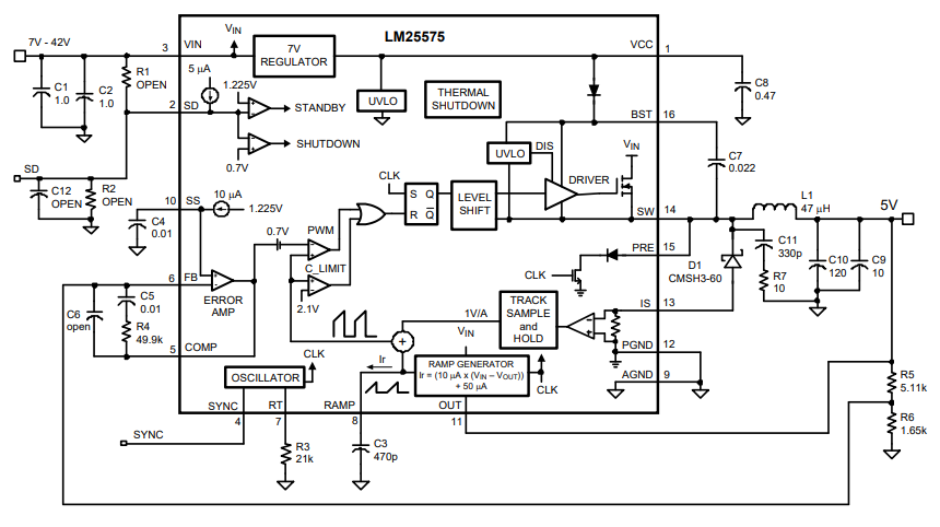
| LM25575MHX/NOPB FUNCTIONAL BLOCK DIAGRAM |
| LM25575MHX/NOPB APPLICATIONS |
|
| COUNTRY OF ORIGIN |
| Malaysia |
|
| PARAMETRIC INFO |
| Type |
Synchronous Step Down |
| Number of Outputs |
1 |
| Minimum Input Voltage (V) |
6 |
| Maximum Input Voltage (V) |
42 |
| Output Voltage (V) |
1.225 to 40 |
| Maximum Output Current (A) |
1.5 |
| Minimum Operating Temperature (°C) |
-40 |
| Maximum Operating Temperature (°C) |
125 |
| Switching Frequency (kHz) |
50 to 1000 |
| Efficiency (%) |
90 |
| Switching Regulator |
Yes |
| Operating Supply Voltage (V) |
6 to 42 |
| Output Type |
Adjustable |
| Typical Quiescent Current (uA) |
1000 |
|
| PACKAGE INFO |
| Supplier Package |
HTSSOP EP |
| Basic Package Type |
Lead-Frame SMT |
| Pin Count |
16 |
| Lead Shape |
Gull-wing |
| PCB |
16 |
| Tab |
N/R |
| Pin Pitch (mm) |
0.65 |
| Package Length (mm) |
5.1(Max) |
| Package Width (mm) |
4.5(Max) |
| Package Height (mm) |
1.05(Max) |
| Package Diameter (mm) |
N/R |
| Package Overall Length (mm) |
5.1(Max) |
| Package Overall Width (mm) |
6.6(Max) |
| Package Overall Height (mm) |
1.2(Max) |
| Seated Plane Height (mm) |
1.2(Max) |
| Mounting |
Surface Mount |
| Package Weight (g) |
N/A |
| Package Material |
Plastic |
| Package Description |
Heat Sinked Thin Shrink Small Outline Package, Exposed Pad |
| Package Family Name |
SOP |
| Jedec |
N/A |
|
| MANUFACTURING INFO |
| MSL |
1 |
| Maximum Reflow Temperature (°C) |
260 |
| Reflow Solder Time (Sec) |
30 |
| Number of Reflow Cycle |
3 |
| Standard |
J-STD-020D |
| Reflow Temp. Source |
Link to Datasheet |
| Maximum Wave Temperature (°C) |
N/R |
| Wave Solder Time (Sec) |
N/R |
| Lead Finish(Plating) |
Matte Sn |
| Under Plating Material |
N/A |
| Terminal Base Material |
Cu Alloy |
| Number of Wave Cycles |
N/R |
|
| PACKAGING INFO |
| Packaging Suffix |
X |
| Packaging |
Tape and Reel |
| Quantity Of Packaging |
2500 |
| Packaging Document |
Link to Datasheet |
|
| ECAD MODELS |
 |
|
| FUNCTIONAL BLOCK DIAGRAM |
 |
|
| APPLICATIONS |
| • Industrial
|
|