 |
|
| • Fully Specified for Operation Over −40°C to 125°C |
| • Output Current in Excess of 500 mA |
| • Output Trimmed for 5% Tolerance Under all Operating Conditions |
| • Typical Dropout Voltage of 0.5 V at Full Rated Load Current |
| • Wide Output Capacitor ESR Range, up to 3 Ω |
| • Internal Short Circuit and Thermal Overload Protection |
| • Reverse Battery Protection |
| • 60-V Input Transient Protection |
| • Mirror Image Insertion Protection |
|
| CATALOG |
| LM2937IMP-5.0/NOPB COUNTRY OF ORIGIN |
| LM2937IMP-5.0/NOPB PARAMETRIC INFO |
| LM2937IMP-5.0/NOPB PACKAGE INFO |
| LM2937IMP-5.0/NOPB MANUFACTURING INFO |
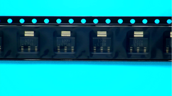
| LM2937IMP-5.0/NOPB PACKAGING INFO |
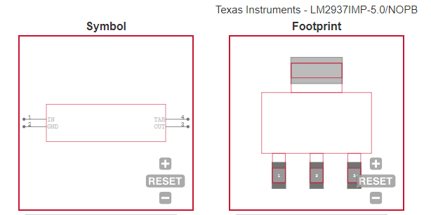
| LM2937IMP-5.0/NOPB ECAD MODELS |
| LM2937IMP-5.0/NOPB FUNCTONAL BLOCK DIAGRAM |
| LM2937IMP-5.0/NOPB APPLICATIONS |
|
| COUNTRY OF ORIGIN |
| China |
| Indonesia |
| Malaysia |
|
| PARAMETRIC INFO |
| Type |
LDO |
| Number of Outputs |
1 |
| Maximum Output Current (A) |
0.5 |
| Minimum Operating Temperature (°C) |
-40 |
| Maximum Operating Temperature (°C) |
85 |
| Output Type |
Fixed |
| Output Voltage Range (V) |
1.8 to 10 |
| Junction to Ambient |
58.3°C/W |
| Junction to Case |
39.2°C/W |
| Polarity |
Positive |
| Special Features |
Short Circuit Protection|Thermal Protection |
| Load Regulation |
50mV |
| Line Regulation |
50mV |
| Maximum Quiescent Current (mA) |
10 |
| Maximum Dropout Voltage @ Current (V) |
0.25@50mA|1@500mA |
| Minimum Input Voltage (V) |
6 |
| Maximum Input Voltage (V) |
26 |
| Output Voltage (V) |
5 |
| Typical Quiescent Current (mA) |
2 |
| Typical Dropout Voltage @ Current (V) |
0.11@50mA|0.5@500mA |
| Accuracy (%) |
±5 |
| Minimum Storage Temperature (°C) |
-65 |
| Maximum Storage Temperature (°C) |
150 |
| Typical PSRR (dB) |
57 |
| Typical Output Noise Voltage (uVrms) |
150 |
|
| PACKAGE INFO |
| Supplier Package |
SOT-223 |
| Basic Package Type |
Lead-Frame SMT |
| Pin Count |
4 |
| Lead Shape |
Gull-wing |
| PCB |
3 |
| Tab |
Tab |
| Pin Pitch (mm) |
2.3 |
| Package Length (mm) |
6.7(Max) |
| Package Width (mm) |
3.7(Max) |
| Package Height (mm) |
1.7(Max) |
| Package Diameter (mm) |
N/R |
| Seated Plane Height (mm) |
1.8(Max) |
| Mounting |
Surface Mount |
| Package Weight (g) |
N/A |
| Package Material |
Plastic |
| Package Description |
Small Outline Transistor |
| Package Family Name |
SOT |
| Jedec |
TO-261AA |
| Package Outline |
Link to Datasheet |
|
| MANUFACTURING INFO |
| MSL |
1 |
| Maximum Reflow Temperature (°C) |
260 |
| Reflow Solder Time (Sec) |
30 |
| Number of Reflow Cycle |
3 |
| Standard |
J-STD-020D |
| Reflow Temp. Source |
Link to Datasheet |
| Maximum Wave Temperature (°C) |
260 |
| Wave Solder Time (Sec) |
4 |
| Wave Temp. Source |
Link to Datasheet |
| Lead Finish(Plating) |
Matte Sn |
| Under Plating Material |
N/A |
| Terminal Base Material |
Cu Alloy |
| Number of Wave Cycles |
N/A |
|
| PACKAGING INFO |
| Packaging |
Tape and Reel |
| Quantity Of Packaging |
1000 |
| Reel Diameter (in) |
13 |
| Reel Width (mm) |
16.4 |
| Tape Pitch (mm) |
12 |
| Tape Width (mm) |
16 |
| Component Orientation |
Q3 |
| Packaging Document |
Link to Datasheet |
|
| ECAD MODELS |
 |
|
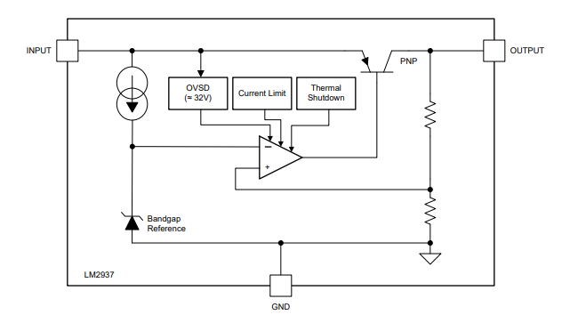
| FUNCTONAL BLOCK DIAGRAM |
|
| APPLICATIONS |
| • Automotive |
| • Industrial Control |
| • Point-of-Load regulation |
|