|
|
• Input Voltage Range = 6 V to 26 V
|
• Dropout Voltage Typically 0.5 V at IOUT = 1 A
|
• Protection Against Inrush Currents
|
• Input UVLO and Output Short-Circuit Protection
|
•–40°C to 125°C Junction Temperature Range
|
•Low Output Voltage Ripple
|
•Fully Enabled for WEBENCH® Power Designer
|
|
| CATALOG |
LM2940CSX-5.0/NOPB COUNTRY OF ORIGIN
|
LM2940CSX-5.0/NOPB PARAMETRIC INFO
|
LM2940CSX-5.0/NOPB PACKAGE INFO
|
LM2940CSX-5.0/NOPB MANUFACTURING INFO
|
LM2940CSX-5.0/NOPB PACKAGING INFO
|
LM2940CSX-5.0/NOPB ECAD MODELS
|
LM2940CSX-5.0/NOPB APPLICATIONS
|
|
COUNTRY OF ORIGIN
|
China
|
Germany
|
Malaysia
|
United Kingdom of Great Britain and Northern Ireland
|
|
PARAMETRIC INFO
|
| Type |
LDO |
| Number of Outputs |
1 |
| Maximum Output Current (A) |
1(Min) |
| Minimum Operating Temperature (°C) |
0 |
| Maximum Operating Temperature (°C) |
125 |
| Output Type |
Fixed |
| Output Voltage Range (V) |
1.8 to 10 |
| Regulation Condition Change In Load |
0.95A |
| Junction to Ambient |
40.9°C/W |
| Junction to Case |
43.5°C/W |
| Polarity |
Positive |
| Special Features |
Current Limit|Reverse Battery Protection|Short Circuit Protection|Shutdown|Thermal Protection |
| Load Regulation |
50mV |
| Line Regulation |
50mV |
| Maximum Quiescent Current (mA) |
15 |
| Maximum Dropout Voltage @ Current (V) |
0.8@1A|0.15@100mA |
| Minimum Input Voltage (V) |
6.25 |
| Maximum Input Voltage (V) |
26 |
| Output Voltage (V) |
5 |
| Typical Quiescent Current (mA) |
10 |
| Typical Dropout Voltage @ Current (V) |
0.11@100mA|0.5@1A |
| Accuracy (%) |
±2 |
| Minimum Storage Temperature (°C) |
-65 |
| Maximum Storage Temperature (°C) |
150 |
| Typical PSRR (dB) |
72 |
| Typical Output Noise Voltage (uVrms) |
150 |
|
|
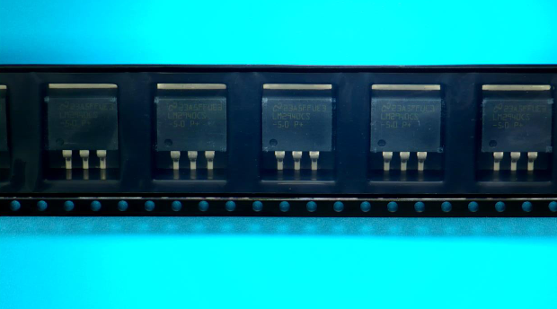
PACKAGE INFO
|
| Supplier Package |
DDPAK |
| Basic Package Type |
Lead-Frame SMT |
| Pin Count |
4 |
| Lead Shape |
Gull-wing |
| PCB |
3 |
| Tab |
Tab |
| Pin Pitch (mm) |
2.54 |
| Package Length (mm) |
10.67(Max) |
| Package Width (mm) |
9.65(Max) |
| Package Height (mm) |
4.83(Max) |
| Package Diameter (mm) |
N/R |
| Package Overall Length (mm) |
10.67(Max) |
| Package Overall Width (mm) |
15.88(Max) |
| Package Overall Height (mm) |
5.08(Max) |
| Seated Plane Height (mm) |
5.08(Max) |
| Mounting |
Surface Mount |
| Package Weight (g) |
N/A |
| Package Material |
Plastic |
| Package Description |
Double Deca Watt Package |
| Package Family Name |
TO-263 |
| Jedec |
TO-263AA |
| Package Outline |
Link to Datasheet |
|
|
MANUFACTURING INFO
|
| MSL |
3 |
| Maximum Reflow Temperature (°C) |
245 |
| Reflow Solder Time (Sec) |
30 |
| Number of Reflow Cycle |
3 |
| Standard |
J-STD-020D |
| Reflow Temp. Source |
Link to Datasheet |
| Maximum Wave Temperature (°C) |
N/R |
| Wave Solder Time (Sec) |
N/R |
| Lead Finish(Plating) |
Matte Sn |
| Under Plating Material |
N/A |
| Terminal Base Material |
Cu Alloy |
| Number of Wave Cycles |
N/R |
|
|
PACKAGING INFO
|
| Packaging Suffix |
X |
| Packaging |
Tape and Reel |
| Quantity Of Packaging |
500 |
| Reel Diameter (in) |
13 |
| Reel Width (mm) |
24.4 |
| Tape Pitch (mm) |
16 |
| Tape Width (mm) |
24 |
| Component Orientation |
Q2 |
| Packaging Document |
Link to Datasheet |
|
|
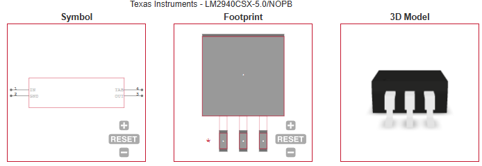
ECAD MODELS
|
|
|
APPLICATIONS
|
• Post Regulator for Switching Supplies
|
| • Logic Power Supplies |
• Industrial Instrumentation
|
|
|
| |