|
|
• Operating VIN Range: 6 V to 26 V
|
• Output Voltage Adjustable From 5 V to 20 V
|
• Dropout Voltage Typically 0.5 V at IOUT = 1 A
|
• Output Current in Excess of 1 A
|
• Trimmed Reference Voltage
|
• Reverse Battery Protection
|
• Internal Short-Circuit Current Limit
|
• Mirror Image Insertion Protection
|
• P
+ Product Enhancement Tested
|
• TTL, CMOS Compatible ON/OFF Switch
|
• Thermal shutdown protection
|
|
| CATALOG |
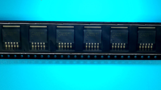
LM2941CSX/NOPB COUNTRY OF ORIGIN
|
LM2941CSX/NOPB PARAMETRIC INFO
|
LM2941CSX/NOPB PACKAGE INFO
|
LM2941CSX/NOPB MANUFACTURING INFO
|
LM2941CSX/NOPB PACKAGING INFO
|
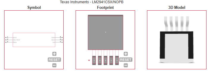
LM2941CSX/NOPB ECAD MODELS
|
LM2941CSX/NOPB APPLICATIONS
|
|
COUNTRY OF ORIGIN
|
Malaysia
|
|
PARAMETRIC INFO
|
| Type |
LDO |
| Number of Outputs |
1 |
| Maximum Output Current (A) |
1(Min) |
| Minimum Operating Temperature (°C) |
0 |
| Maximum Operating Temperature (°C) |
125 |
| Output Type |
Adjustable |
| Output Voltage Range (V) |
1.8 to 10|10 to 20|20 to 50 |
| Polarity |
Positive |
| Special Features |
Current Limit|Reverse Battery Protection|Short Circuit Protection|Thermal Shutdown Protection |
| Load Regulation |
7mV/V(Typ) |
| Line Regulation |
4mV/V(Typ) |
| Maximum Quiescent Current (mA) |
15 |
| Maximum Dropout Voltage @ Current (V) |
0.2@100mA|0.8@1A |
| Minimum Input Voltage (V) |
-15 |
| Maximum Input Voltage (V) |
26 |
| Output Voltage (V) |
5 to 20 |
| Typical Quiescent Current (mA) |
10 |
| Typical Dropout Voltage @ Current (V) |
0.11@100mA|0.5@1A |
| Reference Voltage (V) |
1.313 |
| Minimum Storage Temperature (°C) |
-65 |
| Maximum Storage Temperature (°C) |
150 |
| Typical PSRR (dB) |
67 |
| Typical Output Capacitance (uF) |
22(Min) |
|
|
PACKAGE INFO
|
| Supplier Package |
DDPAK |
| Basic Package Type |
Lead-Frame SMT |
| Pin Count |
6 |
| Lead Shape |
Gull-wing |
| PCB |
5 |
| Tab |
Tab |
| Pin Pitch (mm) |
1.7 |
| Package Length (mm) |
10.67(Max) |
| Package Width (mm) |
9.65(Max) |
| Package Height (mm) |
4.83(Max) |
| Package Diameter (mm) |
N/R |
| Seated Plane Height (mm) |
5.13(Max) |
| Mounting |
Surface Mount |
| Package Weight (g) |
N/A |
| Package Material |
Plastic |
| Package Description |
Double Deca Watt Package |
| Package Family Name |
TO-263 |
| Jedec |
TO-263BA |
| Package Outline |
Link to Datasheet |
|
|
MANUFACTURING INFO
|
| MSL |
3 |
| Maximum Reflow Temperature (°C) |
245 |
| Reflow Solder Time (Sec) |
30 |
| Number of Reflow Cycle |
3 |
| Standard |
J-STD-020D |
| Reflow Temp. Source |
Link to Datasheet |
| Maximum Wave Temperature (°C) |
N/R |
| Wave Solder Time (Sec) |
N/R |
| Lead Finish(Plating) |
Matte Sn |
| Under Plating Material |
N/A |
| Terminal Base Material |
Cu Alloy |
| Number of Wave Cycles |
N/R |
|
|
PACKAGING INFO
|
| Packaging Suffix |
X |
| Packaging |
Tape and Reel |
| Quantity Of Packaging |
500 |
| Reel Diameter (in) |
13 |
| Reel Width (mm) |
24.4 |
| Tape Pitch (mm) |
16 |
| Tape Width (mm) |
24 |
| Component Orientation |
Q2 |
| Packaging Document |
Link to Datasheet |
|
|
ECAD MODELS
|
|
|
APPLICATIONS
|
• Industrial
|
| • Automotive |
|
| |