 |
|
| • Available in 8-bump DSBGA chip-sized package
(see AN-1112, SNVA009)
|
| • Internally frequency compensated for unity gain |
| • Large DC voltage gain: 100 dB |
| • Wide bandwidth (unity gain): 1 MHz (temperature
compensated) |
• Wide power supply range:
– Single supply: 3 V to 32 V
– Or dual supplies: ±1.5 V to ±16 V |
| • Very low supply current drain (500 μA) essentially
independent of supply voltage
|
| • Low input offset voltage: 2 mV |
| • Input common-mode voltage range includes
ground
|
| • Differential input voltage range equal to the power
supply voltage |
| • Large output voltage swing |
• Unique characteristics:
– In the Linear Mode the input common-mode
voltage range includes ground and the output
voltage can also swing to ground, even though
operated from only a single power supply
voltage
– The unity gain cross frequency is temperature
compensated
– The input bias current is also temperature
compensated |
• Advantages:
– Two internally compensated op amps
– Eliminates need for dual supplies
– Allows direct sensing near GND and VOUT also
goes to GND
– Compatible with all forms of logic
– Power drain suitable for battery operation |
|
| CATALOG |
| LM358N/NOPB COUNTRY OF ORIGIN |
| LM358N/NOPB PARAMETRIC INFO |
| LM358N/NOPB PACKAGE INFO |
| LM358N/NOPB MANUFACTURING INFO |
| LM358N/NOPB PACKAGING INFO |
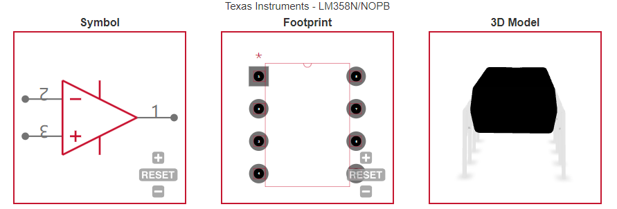
| LM358N/NOPB ECAD MODELS |
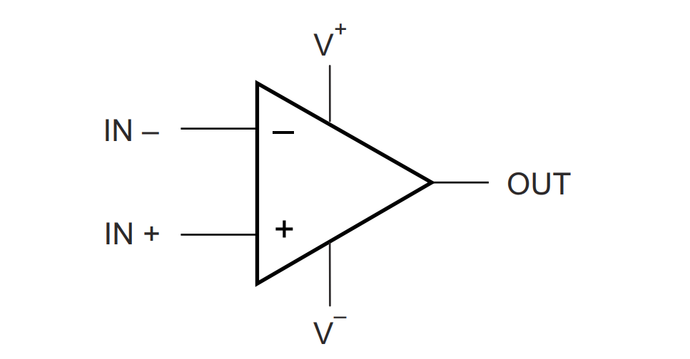
| LM358N/NOPB FUNCTIONAL BLOCK DIAGRAM
|
| LM358N/NOPB APPLICATIONS |
|
| COUNTRY OF ORIGIN |
| Malaysia |
| Philippines |
|
| PARAMETRIC INFO |
| Manufacturer Type |
Low Power Amplifier |
| Type |
Low Power Amplifier |
| Minimum Single Supply Voltage (V) |
3 |
| Number of Channels per Chip |
2 |
| Minimum PSRR (dB) |
65 |
| Typical Single Supply Voltage (V) |
5|9|12|15|18|24|28 |
| Maximum Single Supply Voltage (V) |
32 |
| Maximum Quiescent Current (mA) |
1.2@5V@0C to 70C |
| Minimum Dual Supply Voltage (V) |
±1.5 |
| Typical Gain Bandwidth Product (MHz) |
1 |
| Maximum Input Offset Voltage (mV) |
7@30V |
| Typical Dual Supply Voltage (V) |
±3|±5|±9|±12|±15 |
| Maximum Input Offset Current (uA) |
0.05@5V |
| Maximum Dual Supply Voltage (V) |
±16 |
| Maximum Input Voltage Range (V) |
-0.3 to 32 |
| Maximum Operating Supply Voltage (V) |
±16|32 |
| Maximum Input Bias Current (uA) |
0.25@5V |
| Minimum CMRR (dB) |
65 |
| Maximum Supply Voltage Range (V) |
32 to 36 |
| Minimum CMRR Range (dB) |
65 to 70 |
| Typical Voltage Gain (dB) |
100 |
| Typical Slew Rate (V/us) |
0.1 |
| Typical Output Current (mA) |
40@15V |
| Typical Input Noise Voltage Density (nV/rtHz) |
40@±15V |
| Shut Down Support |
No |
| Minimum Operating Temperature (°C) |
0 |
| Maximum Operating Temperature (°C) |
70 |
| Minimum Storage Temperature (°C) |
-65 |
| Maximum Storage Temperature (°C) |
150 |
| Power Supply Type |
Single|Dual |
| Maximum Power Dissipation (mW) |
830 |
| Input Offset Voltage Drift (uV/°C) |
7 |
|
| |
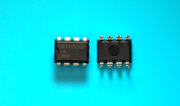
| PACKAGE INFO |
| Supplier Package |
PDIP |
| Basic Package Type |
Through Hole |
| Pin Count |
8 |
| Lead Shape |
Through Hole |
| PCB |
8 |
| Tab |
N/R |
| Pin Pitch (mm) |
2.54 |
| Package Length (mm) |
10.16(Max) |
| Package Width (mm) |
6.6(Max) |
| Package Height (mm) |
5.08(Max) - 0.51(Min) |
| Package Diameter (mm) |
N/R |
| Package Overall Length (mm) |
10.16(Max) |
| Package Overall Width (mm) |
10.92(Max) |
| Package Overall Height (mm) |
5.08(Max) |
| Seated Plane Height (mm) |
5.08(Max) |
| Mounting |
Through Hole |
| Package Weight (g) |
N/A |
| Package Material |
Plastic |
| Package Description |
Plastic Dual In Line Package |
| Package Family Name |
DIP |
| Jedec |
MS-001BA |
| Package Outline |
Link to Datasheet |
|
| |
| MANUFACTURING INFO |
| MSL |
1 |
| Maximum Reflow Temperature (°C) |
N/R |
| Reflow Solder Time (Sec) |
N/R |
| Number of Reflow Cycle |
N/R |
| Standard |
N/R |
| Maximum Wave Temperature (°C) |
260 |
| Wave Solder Time (Sec) |
4 |
| Wave Temp. Source |
Link to Datasheet |
| Lead Finish(Plating) |
Au |
| Under Plating Material |
Pd over Ni |
| Terminal Base Material |
Cu Alloy |
| Number of Wave Cycles |
N/A |
|
| |
| PACKAGING INFO |
| Packaging |
Tube |
| Quantity Of Packaging |
40 |
|
| |
| ECAD MODELS |
 |
|
| FUNCTIONAL BLOCK DIAGRAM
|
 |
|
| APPLICATIONS |
| • Active filters
|
| • General signal conditioning and amplification |
| • 4-mA to 20-mA current loop transmitters
|
| |
|