 |
|
• Wide Supply
– Voltage Range: 2.0 V to 36 V
– Single or Dual Supplies: ±1.0 V to ±18 V |
| • Very Low Supply Current Drain (0.4 mA) —
Independent of Supply Voltage |
| • Low Input Biasing Current: 25 nA |
| • Low Input Offset Current: ±5 nA |
| • Maximum Offset voltage: ±3 mV |
| • Input Common-Mode Voltage Range Includes
Ground |
| • Differential Input Voltage Range Equal to the
Power Supply Voltage
|
| • Low Output Saturation Voltage: 250 mV at 4 mA |
| • Output Voltage Compatible with TTL, DTL, ECL,
MOS and CMOS logic systems |
| • Available in the 8-Bump (12 mil) DSBGA Package |
| • See AN-1112 (SNVA009) for DSBGA
Considerations |
• Advantages
– High Precision Comparators
– Reduced VOS Drift Over Temperature
– Eliminates Need for Dual Supplies
– Allows Sensing Near Ground
– Compatible with All Forms of Logic
– Power Drain Suitable for Battery Operation |
|
| CATALOG |
| LM393MX/NOPB COUNTRY OF ORIGIN |
| LM393MX/NOPB PARAMETRIC INFO |
| LM393MX/NOPB PACKAGE INFO |
| LM393MX/NOPB MANUFACTURING INFO |
| LM393MX/NOPB PACKAGING INFO |
| LM393MX/NOPB ECAD MODELS |
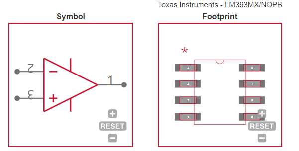
| LM393MX/NOPB FUNCTIONAL BLOCK DIAGRAM |
| LM393MX/NOPB APPLICATIONS |
|
| COUNTRY OF ORIGIN |
| Philippines |
| Malaysia |
|
| PARAMETRIC INFO |
| Rail to Rail |
Rail to Rail Output |
| Manufacturer Type |
Voltage Comparator |
| Number of Channels per Chip |
2 |
| Output Type |
Open Collector |
| Maximum Input Offset Voltage (mV) |
5@30V |
| Maximum Input Bias Current (uA) |
0.25@5V |
| Maximum Input Voltage Range (V) |
-0.3 to 36 |
| Typical Voltage Gain (dB) |
106.02 |
| Typical Voltage Gain Range (dB) |
90 to 110 |
| Strobe Capability |
No |
| Typical Output Current (mA) |
16@5V |
| Typical Input Offset Current (uA) |
0.005@5V |
| Maximum Input Offset Current (uA) |
0.05@5V |
| Typical Response Time (us) |
1.3 |
| Typical Response Time Range (us) |
0.5 to 5 |
| Maximum Propagation Delay Time (ns) |
700(Typ) |
| Minimum Operating Temperature (°C) |
0 |
| Maximum Operating Temperature (°C) |
70 |
| Minimum Storage Temperature (°C) |
-65 |
| Maximum Storage Temperature (°C) |
150 |
| Power Supply Type |
Single|Dual |
| Integrated Voltage Reference |
No |
| Maximum Test Temperature (°C) |
70 |
| Minimum Test Temperature (°C) |
0 |
| Maximum Operating Supply Voltage (V) |
±18|36 |
| Integrated OP Amp |
No |
| Minimum Single Supply Voltage (V) |
2 |
| Typical Single Supply Voltage (V) |
3|5|9|12|15|18|24|28 |
| Maximum Single Supply Voltage (V) |
36 |
| Minimum Dual Supply Voltage (V) |
±1 |
| Typical Dual Supply Voltage (V) |
±3|±5|±9|±12|±15 |
| Maximum Dual Supply Voltage (V) |
±18 |
| Maximum Quiescent Current (mA) |
1@5V |
| Maximum Power Dissipation (mW) |
510 |
|
|
| PACKAGE INFO |
| Supplier Package |
SOIC |
| Basic Package Type |
Lead-Frame SMT |
| Pin Count |
8 |
| Lead Shape |
Gull-wing |
| PCB |
8 |
| Tab |
N/R |
| Pin Pitch (mm) |
1.27 |
| Package Length (mm) |
5(Max) |
| Package Width (mm) |
3.98(Max) |
| Package Height (mm) |
1.5(Max) |
| Package Diameter (mm) |
N/R |
| Package Overall Length (mm) |
5(Max) |
| Package Overall Width (mm) |
6.19(Max) |
| Package Overall Height (mm) |
1.75(Max) |
| Seated Plane Height (mm) |
1.75(Max) |
| Mounting |
Surface Mount |
| Package Weight (g) |
N/A |
| Package Material |
Plastic |
| Package Description |
Small Outline IC |
| Package Family Name |
SO |
| Jedec |
MS-012AA |
| Package Outline |
Link to Datasheet |
|
|
| MANUFACTURING INFO |
| MSL |
1 |
| Maximum Reflow Temperature (°C) |
260 |
| Reflow Solder Time (Sec) |
30 |
| Number of Reflow Cycle |
3 |
| Standard |
J-STD-020D |
| Reflow Temp. Source |
Link to Datasheet |
| Maximum Wave Temperature (°C) |
N/R |
| Wave Solder Time (Sec) |
N/R |
| Lead Finish(Plating) |
Matte Sn |
| Under Plating Material |
N/A |
| Terminal Base Material |
Cu Alloy |
| Number of Wave Cycles |
N/R |
|
|
| PACKAGING INFO |
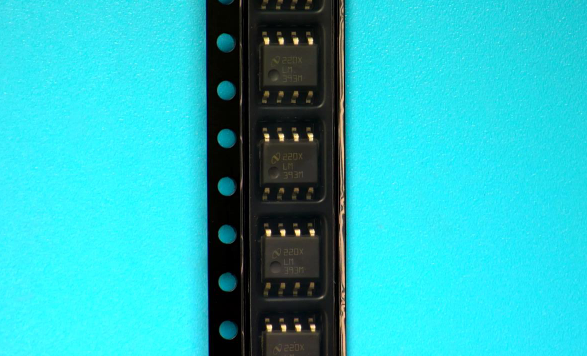
| Packaging Suffix |
X |
| Packaging |
Tape and Reel |
| Quantity Of Packaging |
2500 |
| Reel Diameter (in) |
13 |
| Reel Width (mm) |
12.4 |
| Tape Pitch (mm) |
8 |
| Tape Width (mm) |
12 |
| Component Orientation |
Q1 |
| Packaging Document |
Link to Datasheet |
|
|
| ECAD MODELS |
 |
|
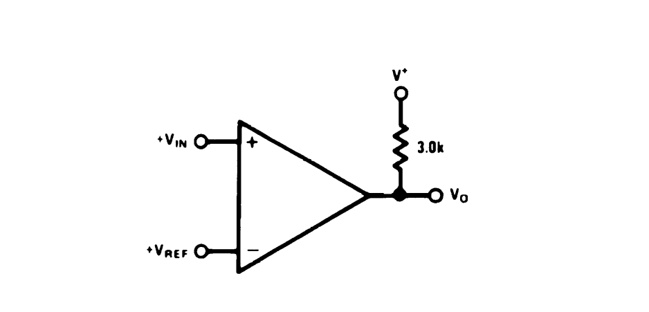
| FUNCTIONAL BLOCK DIAGRAM |
 |
|
| APPLICATIONS |
| • Battery Powered Applications |
| • Industrial Applications |
| |
|