|
|
• LM5010A-Q1 Qualified for AutomotiveApplications
|
• AEC-Q100 Qualified With the Following Results:
– Device Temperature Grade 1: –40°C to 125°CAmbient Operating Temperature Range
– Device Temperature Grade 0: –40°C to 150°CAmbient Operating Temperature Range
– Device HBM ESD Classification Level 2
– Device CDM ESD Classification Level C5
|
• Wide 6-V to 75-V Input Voltage Range
|
• Valley Current Limit at 1.25 A
|
• Programmable Switching Frequency Up To 1 MHz
|
• Integrated 80-V N-Channel Buck Switch
|
• Integrated High Voltage Bias Regulator
|
• No Loop Compensation Required
|
• Ultra-Fast Transient Response
|
• Nearly Constant Operating Frequency With Lineand Load Variations
|
• Adjustable Output Voltage
|
• 2.5-V, ±2% Feedback Reference
|
• Programmable Soft-Start
|
• Thermal Shutdown
|
• Exposed Thermal Pad for Improved HeatDissipation
|
|
| CATALOG |
LM5010ASD/NOPB COUNTRY OF ORIGIN
|
LM5010ASD/NOPB PARAMETRIC INFO
|
LM5010ASD/NOPB PACKAGE INFO
|
LM5010ASD/NOPB MANUFACTURING INFO
|
LM5010ASD/NOPB PACKAGING INFO
|
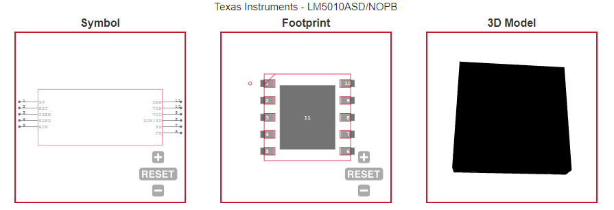
LM5010ASD/NOPB ECAD MODELS
|
LM5010ASD/NOPB FUNCTIONAL BLOCK DIAGRAM
|
LM5010ASD/NOPB APPLICATIONS
|
|
COUNTRY OF ORIGIN
|
Malaysia
|
Thailand
|
|
PARAMETRIC INFO
|
| Type |
Step Down |
| Number of Outputs |
1 |
| Minimum Input Voltage (V) |
6 |
| Maximum Input Voltage (V) |
75 |
| Output Voltage (V) |
2.5 to 70 |
| Maximum Output Current (A) |
1 |
| Minimum Operating Temperature (°C) |
-40 |
| Maximum Operating Temperature (°C) |
150 |
| Switching Frequency (kHz) |
50 to 1000 |
| Efficiency (%) |
91 |
| Switching Regulator |
Yes |
| Operating Supply Voltage (V) |
6 to 75 |
| Output Type |
Adjustable |
| Typical Quiescent Current (uA) |
650 |
| Minimum Storage Temperature (°C) |
-65 |
| Maximum Storage Temperature (°C) |
150 |
|
|
PACKAGE INFO
|
| Supplier Package |
WSON EP |
| Basic Package Type |
Non-Lead-Frame SMT |
| Pin Count |
10 |
| Lead Shape |
No Lead |
| PCB |
10 |
| Tab |
N/R |
| Pin Pitch (mm) |
0.8 |
| Package Length (mm) |
4.1(Max) |
| Package Width (mm) |
4.1(Max) |
| Package Height (mm) |
0.75(Max) |
| Package Diameter (mm) |
N/R |
| Package Overall Length (mm) |
4.1(Max) |
| Package Overall Width (mm) |
4.1(Max) |
| Package Overall Height (mm) |
0.8(Max) |
| Seated Plane Height (mm) |
0.8(Max) |
| Mounting |
Surface Mount |
| Package Material |
Plastic |
| Package Description |
Very Very Thin Small Outline No Lead Package, Exposed Pad |
| Package Family Name |
SON |
| Jedec |
N/A |
|
|
MANUFACTURING INFO
|
| MSL |
1 |
| Maximum Reflow Temperature (°C) |
260 |
| Reflow Solder Time (Sec) |
40 |
| Number of Reflow Cycle |
4 |
| Standard |
IPC-1752 |
| Reflow Temp. Source |
Link to Datasheet |
| Maximum Wave Temperature (°C) |
N/R |
| Wave Solder Time (Sec) |
N/R |
| Lead Finish(Plating) |
Matte Sn|Au |
| Under Plating Material |
N/A|Pd over Ni |
| Terminal Base Material |
Cu Alloy |
|
|
PACKAGING INFO
|
| Packaging |
Tape and Reel |
| Quantity Of Packaging |
1000 |
|
|
ECAD MODELS
|
|
|
FUNCTIONAL BLOCK DIAGRAM
|

|
|
APPLICATIONS
|
• Non-Isolated Telecommunications Regulators
|
• Secondary Side Post Regulators
|
• Automotive Electronics
|
|