 |
|
| • Available in Standard and AEC-Q100 Qualified
Versions LM5050Q0MK-1 (up to 150°C TJ
) and
LM5050Q1MK-1 (up to 125°C TJ
) |
• Functional safety capable
– Documentation available to aid functional
safety system design |
| • Wide Operating Input Voltage Range, VIN: 1 V to
75 V (VBIAS required for VIN < 5 V)
|
| • 100-V Transient Capability |
| • Charge Pump Gate Driver for External N-Channel
MOSFET
|
| • Fast 50-ns Response to Current Reversal
|
| • 2-A Peak Gate Turnoff Current |
| • Minimum VDS Clamp for Faster Turnoff |
| • Package: SOT-6 (Thin SOT-23-6)
|
|
| CATALOG |
| LM5050MK-1/NOPB COUNTRY OF ORIGIN |
| LM5050MK-1/NOPB PARAMETRIC INFO |
| LM5050MK-1/NOPB PACKAGE INFO |
| LM5050MK-1/NOPB MANUFACTURING INFO |
| LM5050MK-1/NOPB PACKAGING INFO |
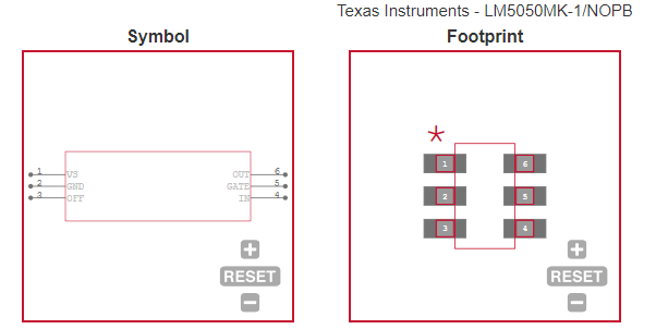
| LM5050MK-1/NOPB ECAD MODELS |
| LM5050MK-1/NOPB FUNCTIONAL BLOCK DIAGRAM |
| LM5050MK-1/NOPB APPLICATIONS |
|
| COUNTRY OF ORIGIN |
| China |
| Malaysia |
|
| PARAMETRIC INFO |
| FET Type |
N-Channel |
| Number of Drivers |
1 |
| Minimum Operating Temperature (°C) |
-40 |
| Maximum Operating Temperature (°C) |
125 |
| Minimum Operating Supply Voltage (V) |
5 |
| Maximum Operating Supply Voltage (V) |
75 |
| Maximum Supply Current (mA) |
0.13(Typ) |
| Maximum Turn-Off Time (ns) |
486(Typ) |
| Minimum Storage Temperature (°C) |
-65 |
| Maximum Storage Temperature (°C) |
150 |
|
|
| PACKAGE INFO |
| Supplier Package |
TSOT-23 |
| Basic Package Type |
Lead-Frame SMT |
| Pin Count |
6 |
| Lead Shape |
Gull-wing |
| PCB |
6 |
| Tab |
N/R |
| Pin Pitch (mm) |
0.95 |
| Package Length (mm) |
3.05(Max) |
| Package Width (mm) |
1.75(Max) |
| Package Height (mm) |
1(Max) |
| Package Diameter (mm) |
N/R |
| Package Overall Length (mm) |
3.05(Max) |
| Package Overall Width (mm) |
3.05(Max) |
| Package Overall Height (mm) |
1.1(Max) |
| Seated Plane Height (mm) |
1.1(Max) |
| Mounting |
Surface Mount |
| Package Weight (g) |
N/A |
| Package Material |
Plastic |
| Package Description |
Thin Small Outline Transistor |
| Package Family Name |
SOT |
| Jedec |
MO-193AA |
| Package Outline |
Link to Datasheet |
|
|
| MANUFACTURING INFO |
| MSL |
1 |
| Maximum Reflow Temperature (°C) |
260 |
| Reflow Solder Time (Sec) |
30 |
| Number of Reflow Cycle |
3 |
| Standard |
J-STD-020D |
| Reflow Temp. Source |
Link to Datasheet |
| Maximum Wave Temperature (°C) |
N/R |
| Wave Solder Time (Sec) |
N/R |
| Lead Finish(Plating) |
Matte Sn |
| Under Plating Material |
N/A |
| Terminal Base Material |
Cu Alloy |
| Number of Wave Cycles |
N/R |
|
| |
| PACKAGING INFO |
| Packaging |
Tape and Reel |
| Quantity Of Packaging |
1000 |
|
|
| ECAD MODELS |
 |
|
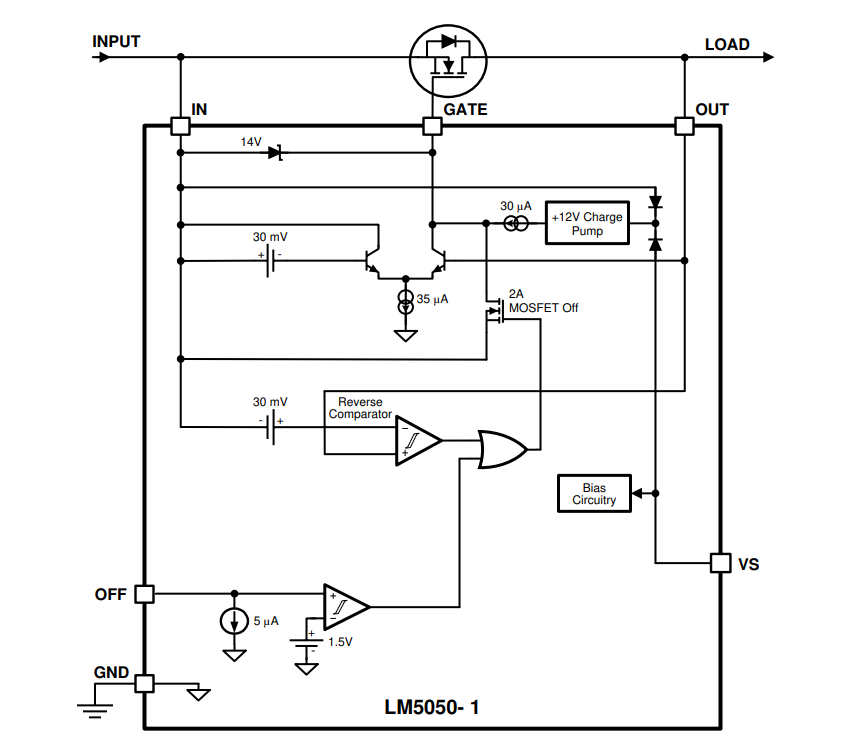
| FUNCTIONAL BLOCK DIAGRAM |
 |
|
| APPLICATIONS |
| Active OR-ing of Redundant (N+1) Power
Supplies |
| |
|