|
|
• 3-A or 2-A Maximum Load Current
|
• Input Voltage Range From 3.5 V to 36 V: Transients to 42 V
|
• Adjustable Output Voltage From 3.3 V to 10 V
|
| • 2.1-MHz Fixed Switching Frequency
|
| • ±2% Output Voltage Tolerance |
| • –40°C to 150°C Junction Temperature Range |
| • 1.7-µA Shutdown Current (Typical) |
| • 24-µA Input Supply Current at No Load (Typical) |
| • Reset Output With Filter and Delay |
| • Automatic Light Load Mode for Improved Efficiency |
| • User-Selectable Forced PWM Mode (FPWM) |
| • Built-In Loop Compensation, Soft-Start, Current Limit, Thermal Shutdown, UVLO, and External Frequency Synchronization |
| • Thermally Enhanced 16-Lead Package:5 mm × 4.4 mm × 1 mm |
| |
| CATALOG |
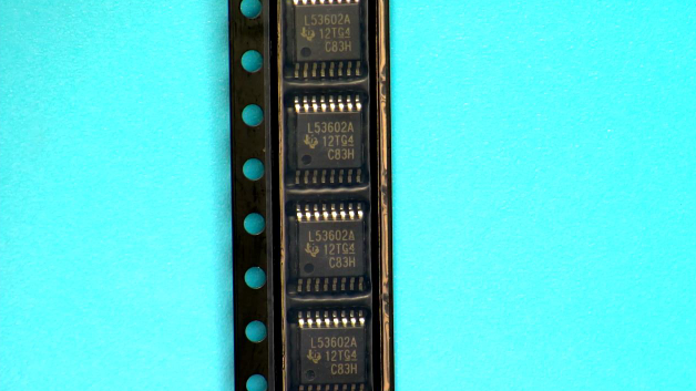
LM53602AMPWPT PARAMETRIC INFO
|
LM53602AMPWPT PACKAGE INFO
|
LM53602AMPWPT MANUFACTURING INFO
|
LM53602AMPWPT PACKAGING INFO
|
LM53602AMPWPT EACD MODELS
|
| LM53602AMPWPT APPLICATIONS |
|
PARAMETRIC INFO
|
| type |
Synchronous Step Down |
| Number of Outputs |
1 |
| Minimum Input Voltage (V) |
3.5 |
| Maximum Input Voltage (V) |
36 |
| Output Voltage (V) |
3.3 to 10 |
| Maximum Output Current (A) |
2 |
| Minimum Operating Temperature (°C) |
-40 |
| Maximum Operating Temperature (°C) |
125 |
| Switching Frequency (kHz) |
2100(Typ) |
| Switching Regulator |
yes |
| Operating Supply Voltage (V) |
3.3 to 10 |
| Output Type |
Adjustable |
| Load Regulation |
77mV(Typ) |
| Line Regulation |
7mV(Typ) |
| Typical Quiescent Current (uA) |
8 |
| Minimum Storage Temperature (°C) |
-40 |
| Maximum Storage Temperature (°C) |
150 |
| Typical Switch Current (A) |
2.4 |
|
|
PACKAGE INFO
|
| Supplier packaging |
HTSSOP EP |
| Basic package type |
Lead-Frame SMT |
| Number of pins |
16 |
| Pin shape |
Gull-wing |
| PCB |
16 |
| ears |
N/R |
| Pin spacing (mm) |
0.65 |
| Package length (mm) |
5.1(Max) |
| Package width (mm) |
4.5(Max) |
| Package height (mm) |
1.05(Max) |
| Package diameter (mm) |
N/R |
| Package Overall Length (mm) |
5.1(Max) |
| Package Overall Width (mm) |
6.6(Max) |
| Package Overall Height (mm) |
1.2(Max) |
| Mounting surface height (mm) |
1.2(Max) |
| Install |
Surface Mount |
| Packaging materials |
Plastic |
| package instruction |
Heat Sinked Thin Shrink Small Outline Package, Exposed Pad |
| Package series name |
SO |
| JEDEC |
not applicable |
|
|
MANUFACTURING INFO
|
| MSL |
3 |
| Maximum reflow temperature (°C) |
260 |
| Reflow soldering time (seconds) |
30 |
| Number of reflow cycles |
3 |
| Reflow temperature source |
Link to datasheet |
| Maximum wave soldering temperature (°C) |
N/R |
| Wave soldering time (seconds) |
N/R |
| Lead Finish(Plating) |
Au |
| Plating materials |
Pd over Ni |
| Terminal Base Material |
Cu |
|
|
PACKAGING INFO
|
| Packaging Suffix |
T |
| Package |
Tape and reel packaging |
| Packing quantity |
250 |
| packaging type file |
Link to datasheet |
|
|
ECAD MODELS
|
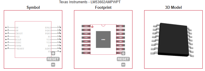
|
|
| APPLICATIONS |
| • Industrial Power Supplies in Building and Factory Automation |
| • Battery Operated Devices |
| • Low-noise and Low-EMI Applications |
| • Optical Communication Systems |
| |