 |
|
• The LM53603-Q1, LM53602-Q1 are available as
AEC-Q1-Qualified Automotive Grade Products
With Following Results:
– Device Temperature Grade 1: -40°C to +125°C
Ambient Operating Range
– Device HBM ESD Classification Level 1C
– Device CDM ESD Classification Level C4B |
| • 3 A or 2 A maximum load current |
| • Input Voltage Range from 3.5 V to 36 V:
Transients to 42 V |
| • Output Voltage Options: 5 V, 3.3 V, ADJ |
| • 2.1 MHz Fixed Switching Frequency |
| • ±2% Output Voltage Tolerance |
| • –40°C to 150°C Junction Temperature Range
|
| • 1.7 µA Shutdown Current (typical) |
| • 24 µA Input Supply Current at No Load (typical)
|
| • No external Feed-back Divider Required for 5 V or
3.3 V output |
| • Reset Output With Filter and Delay |
| • Automatic Light Load Mode for Improved
Efficiency |
| • User-Selectable Forced PWM mode (FPWM) |
| • Built-in Loop Compensation, Soft-start, Current
Limit, Thermal Shutdown, UVLO, and External
Frequency Synchronization |
| • Thermally Enhanced 16-lead Package:
5 mm x 4.4 mm x 1 mm
|
|
| CATALOG |
| LM53602AQPWPRQ1 COUNTRY OF ORIGIN |
| LM53602AQPWPRQ1 PARAMETRIC INFO |
| LM53602AQPWPRQ1 PACKAGE INFO |
| LM53602AQPWPRQ1 MANUFACTURING INFO |
| LM53602AQPWPRQ1 PACKAGING INFO |
| LM53602AQPWPRQ1 ECAD MODELS |
| LM53602AQPWPRQ1 FUNCTIONAL BLOCK DIAGRAM |
| LM53602AQPWPRQ1 APPLICATIONS |
|
| COUNTRY OF ORIGIN |
| Taiwan (Province of China) |
|
| PARAMETRIC INFO |
| Type |
Synchronous Step Down |
| Number of Outputs |
1 |
| Minimum Input Voltage (V) |
3.9 |
| Maximum Input Voltage (V) |
36 |
| Output Voltage (V) |
5|3.3|3.3 to 6 |
| Maximum Output Current (A) |
2 |
| Minimum Operating Temperature (°C) |
-40 |
| Maximum Operating Temperature (°C) |
150 |
| Supplier Temperature Grade |
Automotive |
| Switching Frequency (kHz) |
2350 |
| Switching Regulator |
Yes |
| Operating Supply Voltage (V) |
3.9 to 36 |
| Output Type |
Adjustable|Fixed |
| Load Regulation |
77mV(Typ) |
| Line Regulation |
7mV(Typ) |
| Typical Quiescent Current (uA) |
8 |
| Minimum Storage Temperature (°C) |
-40 |
| Maximum Storage Temperature (°C) |
150 |
| Typical Switch Current (A) |
4.4(Max) |
|
| |
| PACKAGE INFO |
| Supplier Package |
HTSSOP EP |
| Basic Package Type |
Lead-Frame SMT |
| Pin Count |
16 |
| Lead Shape |
Gull-wing |
| PCB |
16 |
| Tab |
N/R |
| Pin Pitch (mm) |
0.65 |
| Package Length (mm) |
5.1(Max) |
| Package Width (mm) |
4.5(Max) |
| Package Height (mm) |
1.05(Max) |
| Package Diameter (mm) |
N/R |
| Package Overall Length (mm) |
5.1(Max) |
| Package Overall Width (mm) |
6.6(Max) |
| Package Overall Height (mm) |
1.2(Max) |
| Seated Plane Height (mm) |
1.2(Max) |
| Mounting |
Surface Mount |
| Package Weight (g) |
N/A |
| Package Material |
Plastic |
| Package Description |
Heat Sinked Thin Shrink Small Outline Package, Exposed Pad |
| Package Family Name |
SO |
| Jedec |
N/A |
|
| |
| MANUFACTURING INFO |
| MSL |
3 |
| Maximum Reflow Temperature (°C) |
260 |
| Reflow Solder Time (Sec) |
30 |
| Number of Reflow Cycle |
3 |
| Standard |
J-STD-020D |
| Reflow Temp. Source |
Link to Datasheet |
| Maximum Wave Temperature (°C) |
N/R |
| Wave Solder Time (Sec) |
N/R |
| Lead Finish(Plating) |
Au |
| Under Plating Material |
Pd over Ni |
| Terminal Base Material |
Cu Alloy |
|
| |
| PACKAGING INFO |
| Packaging Suffix |
R |
| Packaging |
Tape and Reel |
| Quantity Of Packaging |
2000 |
| Packaging Document |
Link to Datasheet |
|
| |
| ECAD MODELS |
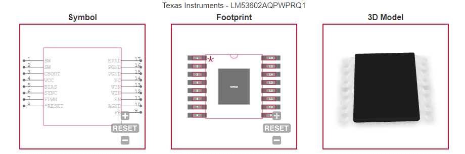 |
|
| FUNCTIONAL BLOCK DIAGRAM |
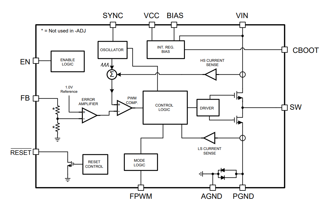 |
|
| APPLICATIONS |
| • Navigation/GPS |
| • Instrument Cluster |
| • ADAS, Infotainment, HUD |
|