|
|
• Wide Supply Voltage Range 2.5 V to 32 V
|
• Output Current +65 mA/−100 mA
|
• Gain Bandwidth Product 20 MHz
|
| • Slew Rate 18 V/µs
|
| • Capacitive Load Tolerance Unlimited |
| • Input Common-Mode Voltage 0.3-V Beyond Rails |
| • Input Voltage Noise 15 nV/√Hz |
| • Input Current Noise 1.3 pA/√Hz |
| • Supply Current/Channel 1.1 mA |
| • Distortion THD+Noise −86 dB |
| • Temperature Range −40°C to 125°C |
• Tested at −40°C, 25°C and 125°C at 2.7 V, ±5 V,+-15V
|
|
| CATALOG |
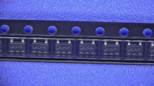
| LM7321MF/NOPB COUNTRY OF ORIGIN |
| LM7321MF/NOPB LIFE CYCLE |
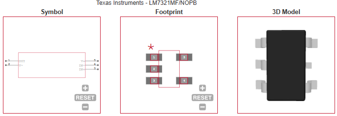
LM7321MF/NOPB PARAMETRIC INFO
|
LM7321MF/NOPB PACKAGE INFO
|
LM7321MF/NOPB MANUFACTURING INFO
|
LM7321MF/NOPB PACKAGING INFO
|
LM7321MF/NOPB EACD MODELS
|
| LM7321MF/NOPB APPLICATIONS |
|
| COUNTRY OF ORIGIN |
| Malaysia |
|
| LIFE CYCLE |
| LTB May 22, 2024 |
| |
PARAMETRIC INFO
|
| Manufacturer Type |
High Output Current Amplifier |
| type |
High Output Current Amplifier |
| Rail to Rail |
Rail to Rail Input/Output |
| Minimum Single Supply Voltage (V) |
2.5 |
| Number of Channels per Chip |
1 |
| Minimum PSRR (dB) |
78 |
| Typical Single Supply Voltage (V) |
2.7 |
| Maximum Single Supply Voltage (V) |
32 |
| Minimum Dual Supply Voltage (V) |
±1.25 |
| Typical Gain Bandwidth Product (MHz) |
16 |
| Maximum Input Offset Voltage (mV) |
5@±5V |
| Typical Dual Supply Voltage (V) |
±5|±15 |
| Maximum Input Offset Current (uA) |
0.2@±5V |
| Maximum Dual Supply Voltage (V) |
±16 |
| Maximum Operating Supply Voltage (V) |
±16|32 |
| Maximum Input Bias Current (uA) |
1@±5V |
| Minimum CMRR (dB) |
65 |
| Maximum Supply Voltage Range (V) |
32 to 36 |
| Minimum CMRR Range (dB) |
65 to 70 |
| Typical Voltage Gain (dB) |
80 |
| Typical Slew Rate (V/us) |
12.3@±5V |
| Typical Input Offset Current (uA) |
0.02@±5V |
| Typical Output Current (mA) |
85@±5V |
| Typical Input Noise Voltage Density (nV/rtHz) |
14.3@±5V |
| Typical Noninverting Input Current Noise Density (pA/rtHz) |
1.35@±5V |
| Typical Input Bias Current (uA) |
0.45@±5V |
| Shut Down Support |
no |
| Minimum Operating Temperature (°C) |
-40 |
| Maximum Operating Temperature (°C) |
125 |
| Minimum Storage Temperature (°C) |
-65 |
| Maximum Storage Temperature (°C) |
150 |
| Power Supply Type |
Single|Dual |
| Maximum Supply Current (mA) |
1.3@±5V |
| Typical High Level Output Voltage (V) |
0.16 |
| Typical Low Level Output Voltage (V) |
0.08 |
| Input Offset Voltage Drift (uV/°C) |
±2(Typ) |
|
|
PACKAGE INFO
|
| Supplier packaging |
SOT-23 |
| Basic package type |
Lead-Frame SMT |
| Number of pins |
5 |
| Pin shape |
Gull-wing |
| PCB |
5 |
| ears |
N/R |
| Pin spacing (mm) |
0.95 |
| Package length (mm) |
3.05(Max) |
| Package width (mm) |
1.75(Max) |
| Package height (mm) |
1.1 |
| Package diameter (mm) |
N/R |
| Package Overall Length (mm) |
3.05(Max) |
| Package Overall Width (mm) |
3(Max) |
| Package Overall Height (mm) |
1.45(Max) |
| Mounting surface height (mm) |
1.45(Max) |
| Install |
Surface Mount |
| Package weight (g) |
not applicable |
| Packaging materials |
Plastic |
| package instruction |
Small Outline Transistor |
| Package series name |
SOT |
| JEDEC |
MO-178AA |
| Package outline |
Link to datasheet |
|
|
MANUFACTURING INFO
|
| MSL |
1 |
| Maximum reflow temperature (°C) |
260 |
| Reflow soldering time (seconds) |
30 |
| Number of reflow cycles |
3 |
| standard |
J-STD-020D |
| Reflow temperature source |
Link to datasheet |
| Maximum wave soldering temperature (°C) |
N/R |
| Wave soldering time (seconds) |
N/R |
| Lead Finish(Plating) |
Matt Sn |
| Plating materials |
not applicable |
| Terminal Base Material |
Cu Alloy |
|
|
PACKAGING INFO
|
| Package |
Tape and reel packaging |
| Packing quantity |
1000 |
| Reel Diameter (in) |
7 |
| Reel Width (mm) |
8.4 |
| Tape Pitch (mm) |
4 |
| Tape Width (mm) |
8 |
| Component Orientation |
Q3 |
| packaging type file |
Link to datasheet |
|
|
ECAD MODELS
|
|
|
| APPLICATIONS |
| • Driving MOSFETs and Power Transistors |
| • Capacitive Proximity Sensors |
| • Driving Analog Optocouplers |
| • High-Side Sensing |
| • Below Ground Current Sensing |
| • Photodiode Biasing |
| • Driving Varactor Diodes in PLLs |
| • Wide Voltage Range Power supplies |
| • Automotive |
| • International Power Supplies |
| |