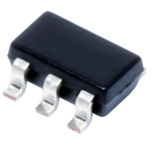
LM7321MFX/NOPB Texas Instruments LM7321x Single and LM7322x Dual Rail-to-Rail Input and Output ±15-V, High-Output Current and Unlimited Capacitive Load Operational Amplifier

label:
2025/05/14 3
LM7321MFX/NOPB Texas Instruments LM7321x Single and LM7322x Dual Rail-to-Rail Input and Output ±15-V, High-Output Current and Unlimited Capacitive Load Operational Amplifier


• Wide Supply Voltage Range 2.5 V to 32 V
• Output Current +65 mA/−100 mA
• Gain Bandwidth Product 20 MHz
• Slew Rate 18 V/µs
• Capacitive Load Tolerance Unlimited
• Input Common-Mode Voltage 0.3-V Beyond Rails
• Input Voltage Noise 15 nV/√Hz


CATALOG
LM7321MFX/NOPB COUNTRY OF ORIGIN
LM7321MFX/NOPB PARAMETRIC INFO
LM7321MFX/NOPB PACKAGE INFO
LM7321MFX/NOPB MANUFACTURING INFO
LM7321MFX/NOPB PACKAGING INFO
LM7321MFX/NOPB ECAD MODELS
LM7321MFX/NOPB APPLICATIONS


COUNTRY OF ORIGIN
Malaysia
Philippines
China


PARAMETRIC INFO
Manufacturer Type High Output Current Amplifier
Type High Output Current Amplifier
Rail to Rail Rail to Rail Input/Output
Number of Channels per Chip 1
Minimum Single Supply Voltage (V) 2.5
Minimum PSRR (dB) 78
Typical Single Supply Voltage (V) 2.7
Maximum Single Supply Voltage (V) 32
Typical Gain Bandwidth Product (MHz) 16
Minimum Dual Supply Voltage (V) ±1.25
Typical Dual Supply Voltage (V) ±5|±15
Maximum Input Offset Voltage (mV) 5@±5V
Maximum Dual Supply Voltage (V) ±16
Maximum Input Offset Current (uA) 0.2@±5V
Maximum Input Bias Current (uA) 1@±5V
Maximum Operating Supply Voltage (V) ±16|32
Maximum Supply Voltage Range (V) 32 to 36
Minimum CMRR (dB) 65
Minimum CMRR Range (dB) 65 to 70
Typical Voltage Gain (dB) 80
Typical Input Offset Current (uA) 0.02@±5V
Typical Slew Rate (V/us) 12.3@±5V
Typical Output Current (mA) 85@±5V
Typical Input Noise Voltage Density (nV/rtHz) 14.3@±5V
Typical Input Bias Current (uA) 0.45@±5V
Typical Noninverting Input Current Noise Density (pA/rtHz) 1.35@±5V
Shut Down Support No
Minimum Operating Temperature (°C) -40
Maximum Operating Temperature (°C) 125
Minimum Storage Temperature (°C) -65
Maximum Storage Temperature (°C) 150
Power Supply Type Single|Dual
Maximum Supply Current (mA) 1.3@±5V
Typical High Level Output Voltage (V) 0.16
Typical Low Level Output Voltage (V) 0.08
Input Offset Voltage Drift (uV/°C) ±2(Typ)


PACKAGE INFO
Supplier Package SOT-23
Basic Package Type Lead-Frame SMT
Pin Count 5
Lead Shape Gull-wing
PCB 5
Tab N/R
Pin Pitch (mm) 0.95
Package Length (mm) 3.05(Max)
Package Width (mm) 1.75(Max)
Package Height (mm) 1.1
Package Diameter (mm) N/R
Package Overall Length (mm) 3.05(Max)
Package Overall Width (mm) 3(Max)
Package Overall Height (mm) 1.45(Max)
Seated Plane Height (mm) 1.45(Max)
Mounting Surface Mount
Package Weight (g) N/A
Package Material Plastic
Package Description Small Outline Transistor
Package Family Name SOT
Jedec MO-178AA
Package Outline Link to Datasheet
Maximum PACKAGE_DIMENSION_H 1.3
Minimum PACKAGE_DIMENSION_H 0.9
Maximum PACKAGE_DIMENSION_L 3.05
Minimum PACKAGE_DIMENSION_L 2.75
Maximum PACKAGE_DIMENSION_W 1.75
Minimum PACKAGE_DIMENSION_W 1.45
Maximum Diameter N/R
Minimum Diameter N/R
Maximum Seated_Plane_Height 1.45
Minimum Seated_Plane_Height 0.9


MANUFACTURING INFO
MSL 1
Maximum Reflow Temperature (°C) 260
Reflow Solder Time (Sec) 30
Number of Reflow Cycle 3
Standard J-STD-020D
Reflow Temp. Source Link to Datasheet
Maximum Wave Temperature (°C) 260
Wave Solder Time (Sec) 4
Wave Temp. Source Link to Datasheet
Lead Finish(Plating) Matte Sn
Under Plating Material N/A
Terminal Base Material Cu Alloy
Number of Wave Cycles N/A


PACKAGING INFO
Packaging Suffix X
Packaging Tape and Reel
Quantity Of Packaging 3000
Reel Diameter (in) 7
Reel Width (mm) 8.4
Tape Pitch (mm) 4
Tape Width (mm) 8
Component Orientation Q3
Packaging Document Link to Datasheet
 
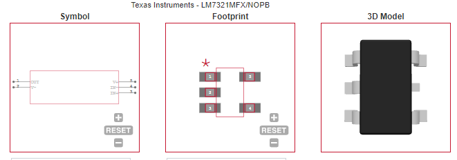
ECAD MODELS


APPLICATIONS
• Driving MOSFETs and Power Transistors
• Capacitive Proximity Sensors
• Driving Analog Optocouplers
• High-Side Sensing
• Below Ground Current Sensing
• Photodiode Biasing
• Driving Varactor Diodes in PLLs
• Wide Voltage Range Power supplies
• Automotive
• International Power Supplies
Продукт RFQ