|
|
• VS = ±15 V, TA = 25°C, Typical Values Unless Specified
|
• Wide Supply Voltage Range 2.5 V to 32 V
|
• Wide Input Common Mode Voltage 0.3 V Beyond Rails
|
| • Output Short Circuit Current > 100 mA
|
| • High Output Current (1 V from Rails) ±70 mA |
| • GBWP 21 MHz |
| • Slew Rate 15.2 V/µs |
| • Capacitive Load Tolerance Unlimited |
| • Total Supply Current 2 mA |
| • Temperature Range −40°C to +125°C |
| • Tested at −40°C, +125°C,and +25°C at 5 V, ±5 V, ±15 V |
|
| CATALOG |
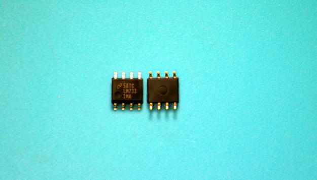
| LM7332MA/NOPB COUNTRY OF ORIGIN |
LM7332MA/NOPB PARAMETRIC INFO
|
LM7332MA/NOPB PACKAGE INFO
|
LM7332MA/NOPB MANUFACTURING INFO
|
LM7332MA/NOPB PACKAGING INFO
|
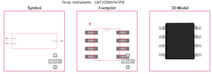
LM7332MA/NOPB EACD MODELS
|
| LM7332MA/NOPB APPLICATIONS |
|
| COUNTRY OF ORIGIN |
| Malaysia |
|
PARAMETRIC INFO
|
| Manufacturer Type |
High Output Power Amplifier |
| type |
High Output Power Amplifier |
| Rail to Rail |
Rail to Rail Input/Output |
| Minimum Single Supply Voltage (V) |
2.5 |
| Number of Channels per Chip |
2 |
| Minimum PSRR (dB) |
78 |
| Typical Single Supply Voltage (V) |
3|5|9|12|15|18|24|28 |
| Maximum Single Supply Voltage (V) |
32 |
| Maximum Quiescent Current (mA) |
2.3@5V |
| Minimum Dual Supply Voltage (V) |
±1.25 |
| Typical Gain Bandwidth Product (MHz) |
19.3 |
| Maximum Input Offset Voltage (mV) |
4@5V |
| Typical Dual Supply Voltage (V) |
±3|±5|±9|±12|±15 |
| Maximum Input Offset Current (uA) |
0.25@5V |
| Maximum Dual Supply Voltage (V) |
±16 |
| Maximum Operating Supply Voltage (V) |
±16|32 |
| Maximum Input Bias Current (uA) |
2@5V |
| Minimum CMRR (dB) |
62 |
| Maximum Supply Voltage Range (V) |
32 to 36 |
| Minimum CMRR Range (dB) |
60 to 65 |
| Typical Voltage Gain (dB) |
77 |
| Typical Slew Rate (V/us) |
12@5V |
| Typical Output Current (mA) |
55@5V |
| Typical Input Noise Voltage Density (nV/rtHz) |
14.8@5V |
| Typical Noninverting Input Current Noise Density (pA/rtHz) |
1.35@5V |
| Typical Input Bias Current (uA) |
1@5V |
| Shut Down Support |
no |
| Minimum Operating Temperature (°C) |
-40 |
| Maximum Operating Temperature (°C) |
125 |
| Minimum Storage Temperature (°C) |
-65 |
| Maximum Storage Temperature (°C) |
150 |
| Power Supply Type |
Single|Dual |
| Typical Output Resistance (Ohm) |
3 |
| Input Offset Voltage Drift (uV/°C) |
2(Typ) |
|
|
PACKAGE INFO
|
| Supplier packaging |
SOIC |
| Basic package type |
Lead-Frame SMT |
| Number of pins |
8 |
| Pin shape |
Gull-wing |
| PCB |
8 |
| ears |
N/R |
| Pin spacing (mm) |
1.27 |
| Package length (mm) |
5(Max) |
| Package width (mm) |
3.98(Max) |
| Package height (mm) |
1.5(Max) |
| Package diameter (mm) |
N/R |
| Package Overall Length (mm) |
5(Max) |
| Package Overall Width (mm) |
6.19(Max) |
| Package Overall Height (mm) |
1.75(Max) |
| Mounting surface height (mm) |
1.75(Max) |
| Install |
Surface Mount |
| Package weight (g) |
not applicable |
| Packaging materials |
Plastic |
| package instruction |
Small Outline IC |
| Package series name |
SO |
| JEDEC |
MS-012AA |
| Package outline |
Link to datasheet |
|
|
MANUFACTURING INFO
|
| MSL |
1 |
| Maximum reflow temperature (°C) |
260 |
| Reflow soldering time (seconds) |
30 |
| Number of reflow cycles |
3 |
| standard |
J-STD-020D |
| Reflow temperature source |
Link to datasheet |
| Maximum wave soldering temperature (°C) |
N/R |
| Wave soldering time (seconds) |
N/R |
| Lead Finish(Plating) |
Matt Sn |
| Plating materials |
not applicable |
| Terminal Base Material |
Cu Alloy |
|
|
PACKAGING INFO
|
| Package |
Tube |
| Packing quantity |
95 |
| packaging type file |
Link to datasheet |
|
|
ECAD MODELS
|
|
|
| APPLICATIONS |
| • MOSFET and Power Transistor Driver |
| • Replaces Discrete Transistors in High Current Output Circuits |
| • Instrumentation 4–20 mA Current Loops |
| • Analog Data Transmission |
| • Multiple Voltage Power Supplies and Battery Chargers |
| • High-Side and Low-Side Current Sensing |
| • Bridge and Sensor Driving |
| • Digital-to-Analog Converter Output |
| |