|
|
• AEC-Q100 grade 1 qualified
|
• 1.25ns typical minimum input pulse width
|
• 2.6ns typical rising propagation delay
|
• 2.9ns typical falling propagation delay
|
• 300ps typical pulse distortion
|
• Independent 7A pull-up and 5A pull-down current
|
|
| CATALOG |
LMG1025QDEERQ1 COUNTRY OF ORIGIN
|
LMG1025QDEERQ1 PARAMETRIC INFO
|
LMG1025QDEERQ1 PACKAGE INFO
|
LMG1025QDEERQ1 MANUFACTURING INFO
|
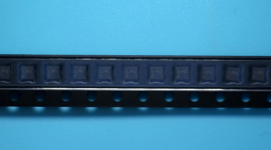
LMG1025QDEERQ1 PACKAGING INFO
|
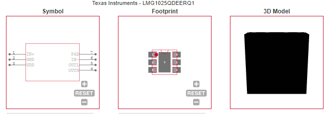
LMG1025QDEERQ1 ECAD MODELS
|
LMG1025QDEERQ1 APPLICATIONS
|
|
COUNTRY OF ORIGIN
|
Thailand
|
|
PARAMETRIC INFO
|
| Driver Type |
Low Side |
| Number of Drivers |
1 |
| Driver Configuration |
Inverting|Non-Inverting |
| Input Logic Compatibility |
CMOS|TTL |
| Maximum Operating Supply Voltage (V) |
5.25 |
| Peak Output Current (A) |
7(Typ) |
| Minimum Operating Temperature (°C) |
-40 |
| Type |
GaNFET|MOSFET |
| Maximum Operating Temperature (°C) |
125 |
| Maximum Turn-Off Delay Time (ns) |
4.4 |
| Maximum Turn-On Delay Time (ns) |
4.1 |
| Number of Outputs |
1 |
| Minimum Operating Supply Voltage (V) |
4.75 |
| Typical Operating Supply Voltage (V) |
5 |
| Maximum Supply Current (mA) |
51(Typ) |
| Supplier Temperature Grade |
Automotive |
| Absolute Propagation Delay Time (ns) |
4.4 |
| Maximum Propagation Delay Time (ns) |
4.4 |
| Maximum Rise Time (ns) |
0.65(Typ) |
| Maximum Fall Time (ns) |
0.85(Typ) |
| Typical Input High Threshold Voltage (V) |
1.7(Min) |
| Typical Input Low Threshold Voltage (V) |
1.8(Max) |
| Latch-Up Proof |
No |
| Special Features |
Under Voltage Lockout|Over Temperature Protection |
| Minimum Storage Temperature (°C) |
-55 |
| Maximum Storage Temperature (°C) |
150 |
|
|
PACKAGE INFO
|
| Supplier Package |
WSON EP |
| Basic Package Type |
Non-Lead-Frame SMT |
| Pin Count |
6 |
| Lead Shape |
No Lead |
| PCB |
6 |
| Tab |
N/R |
| Pin Pitch (mm) |
0.65 |
| Package Length (mm) |
2.1(Max) |
| Package Width (mm) |
2.1(Max) |
| Package Height (mm) |
0.75(Max) |
| Package Diameter (mm) |
N/R |
| Seated Plane Height (mm) |
0.8(Max) |
| Mounting |
Surface Mount |
| Terminal Width (mm) |
0.45(Max) |
| Package Weight (g) |
N/A |
| Package Material |
Plastic |
| Package Description |
Very Very Thin Small Outline No Lead Package, Exposed Pad |
| Package Family Name |
SON |
| Jedec |
N/A |
| Package Outline |
Link to Datasheet |
| Maximum PACKAGE_DIMENSION_L |
2.1 |
| Minimum PACKAGE_DIMENSION_L |
1.9 |
| Maximum PACKAGE_DIMENSION_W |
2.1 |
| Minimum PACKAGE_DIMENSION_W |
1.9 |
| Maximum Diameter |
N/R |
| Minimum Diameter |
N/R |
| Minimum Seated_Plane_Height |
N/A |
| Minimum PACKAGE_DIMENSION_H |
N/A |
| Maximum PACKAGE_DIMENSION_H |
0.75 |
| Maximum Seated_Plane_Height |
0.8 |
|
|
MANUFACTURING INFO
|
| MSL |
2 |
| Maximum Reflow Temperature (°C) |
260 |
| Reflow Solder Time (Sec) |
30 |
| Number of Reflow Cycle |
3 |
| Standard |
J-STD-020D |
| Reflow Temp. Source |
Link to Datasheet |
| Maximum Wave Temperature (°C) |
N/R |
| Wave Solder Time (Sec) |
N/R |
| Wave Temp. Source |
Link to Datasheet |
| Lead Finish(Plating) |
Matte Sn |
| Under Plating Material |
N/A |
| Terminal Base Material |
Cu Alloy |
| Number of Wave Cycles |
N/R |
|
|
| PACKAGING INFO |
| Packaging Suffix |
R |
| Packaging |
Tape and Reel |
| Quantity Of Packaging |
3000 |
| Reel Diameter (in) |
7.09 |
| Reel Width (mm) |
8.4 |
| Tape Pitch (mm) |
4 |
| Tape Width (mm) |
8 |
| Component Orientation |
Q2 |
| Packaging Document |
Link to Datasheet |
|
| |
| ECAD MODELS |
 |
|
| APPLICATIONS |
| • Automotive LIDAR |
| • Driver monitoring |
| • Vehicle occupant detection sensor |
| • DC/DC converter |
| |