|
|
• 24-Bit, Low-Power Sigma-Delta ADC
|
• True Continuous Background Calibration at all Gains
|
• In-Place System Calibration Using Expected Value Programming
|
• Low-Noise Programmable Gain (1x to 128x)
|
• Continuous Background Open / Short and Out-ofRange Sensor Diagn
|
• 8 Output Data Rates (ODR) With Single-Cycle Settling
|
• 2 Matched Excitation Current Sources From 100 µA to 1000 µA (LMP90100/LMP90098)
|
• 4-DIFF / 7-SE Inputs (LMP90100/LMP90099)
|
• 2-DIFF / 4-SE Inputs (LMP90098/LMP90097)
|
|
| CATALOG |
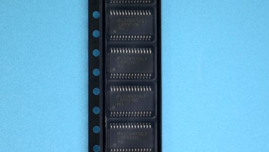
LMP90100MHX/NOPB COUNTRY OF ORIGIN
|
LMP90100MHX/NOPB PARAMETRIC INFO
|
LMP90100MHX/NOPB PACKAGE INFO
|
LMP90100MHX/NOPB MANUFACTURING INFO
|
LMP90100MHX/NOPB PACKAGING INFO
|
LMP90100MHX/NOPB ECAD MODELS
|
LMP90100MHX/NOPB APPLICATIONS
|
|
COUNTRY OF ORIGIN
|
Taiwan (Province of China)
|
Malaysia
|
|
PARAMETRIC INFO
|
| Category |
General Purpose |
| Type |
General Purpose |
| Number of ADCs |
1 |
| Resolution (bit) |
24 |
| Number of Channels per Chip |
1 |
| Number of ADC Inputs |
1 |
| Interface Type |
Serial (SPI) |
| Minimum Operating Temperature (°C) |
-40 |
| Maximum Operating Temperature (°C) |
125 |
| Minimum Storage Temperature (°C) |
-65 |
| Maximum Storage Temperature (°C) |
150 |
| Power Supply Type |
Analog|Digital |
| Minimum Operating Supply Voltage (V) |
2.7|2.85 |
| Typical Operating Supply Voltage (V) |
3.3|5 |
| Maximum Operating Supply Voltage (V) |
5.5 |
| Typical Supply Current (mA) |
1.5 |
|
|
PACKAGE INFO
|
| Supplier Package |
HTSSOP EP |
| Basic Package Type |
Lead-Frame SMT |
| Pin Count |
28 |
| Lead Shape |
Gull-wing |
| PCB |
28 |
| Tab |
N/R |
| Pin Pitch (mm) |
0.65 |
| Package Length (mm) |
9.8(Max) |
| Package Width (mm) |
4.5(Max) |
| Package Height (mm) |
1.05(Max) |
| Package Diameter (mm) |
N/R |
| Package Overall Length (mm) |
9.8(Max) |
| Package Overall Width (mm) |
6.6(Max) |
| Package Overall Height (mm) |
1.2(Max) |
| Seated Plane Height (mm) |
1.2(Max) |
| Mounting |
Surface Mount |
| Package Weight (g) |
N/A |
| Package Material |
Plastic |
| Package Description |
Heat Sinked Thin Shrink Small Outline Package, Exposed Pad |
| Package Family Name |
SO |
| Jedec |
N/A |
| Package Outline |
Link to Datasheet |
|
|
MANUFACTURING INFO
|
| MSL |
3 |
| Maximum Reflow Temperature (°C) |
260 |
| Reflow Solder Time (Sec) |
30 |
| Number of Reflow Cycle |
3 |
| Standard |
J-STD-020D |
| Reflow Temp. Source |
Link to Datasheet |
| Maximum Wave Temperature (°C) |
N/R |
| Wave Solder Time (Sec) |
N/R |
| Lead Finish(Plating) |
Matte Sn |
| Under Plating Material |
N/A |
| Terminal Base Material |
Cu Alloy |
|
|
PACKAGING INFO
|
| Packaging |
Tape and Reel |
| Quantity Of Packaging |
2500 |
| Packaging Document |
Link to Datasheet |
|
|
| ECAD MODELS |

|
|
| APPLICATIONS |
| • Temperature and Pressure Transmitters |
| • Strain Gauge Interface |
| • Industrial Process Control |
| |