 |
|
| • Qualified for Automotive Applications |
• AEC-Q100 Qualified With the Following Results:
- Device Temperature Grade 1: -40 °C to 125 °C
Ambient Operating Temperature Range
- Device HBM ESD Classification Level H1C
- Device CDM ESD Classification Level C4A
|
| • 4 V to 40 V Input Range |
| • 2 A Continuous Output Current |
| • Ultra-low 40 µA Operating Quiescent Current |
| • 90 mΩ High-Side MOSFET
|
| • Minimum Switch-On Time: 75 ns |
| • Current Mode Control
|
| • Adjustable Switching Frequency from 200 kHz to
2.5 MHz |
| • Frequency Synchronization to External Clock
|
| • Spread Spectrum Option for Reduced EMI |
| • Internal Compensation for Ease of Use |
| • High Duty Cycle Operation Supported |
| • Precision Enable Input |
| • 1 µA Shutdown Current |
| • External Soft-start |
| • Thermal, Overvoltage and Short Protection |
|
| CATALOG |
| LMR14020QDPRTQ1 COUNTRY OF ORIGIN |
| LMR14020QDPRTQ1 PARAMETRIC INFO |
| LMR14020QDPRTQ1 PACKAGE INFO |
| LMR14020QDPRTQ1 MANUFACTURING INFO |
| LMR14020QDPRTQ1 PACKAGING INFO |
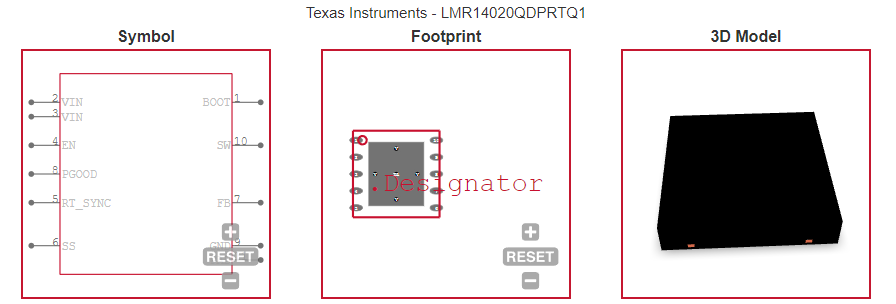
| LMR14020QDPRTQ1 ECAD MODELS |
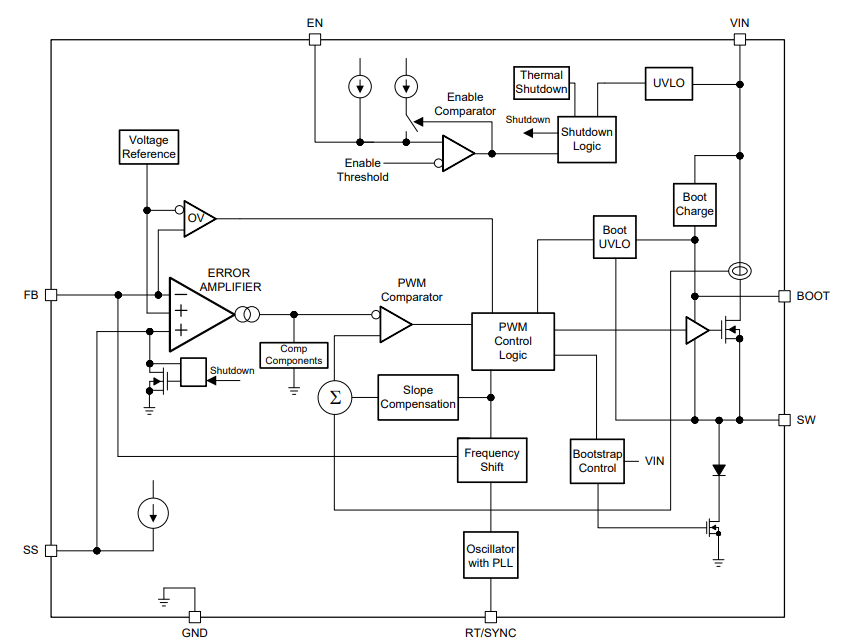
| LMR14020QDPRTQ1 FUNCTIONAL BLOCK DIAGRAM |
| LMR14020QDPRTQ1 APPLICATIONS
|
|
| COUNTRY OF ORIGIN |
| Philippines |
|
| PARAMETRIC INFO |
| Type |
Step Down |
| Number of Outputs |
1 |
| Minimum Input Voltage (V) |
4 |
| Maximum Input Voltage (V) |
40 |
| Output Voltage (V) |
0.8 to 28 |
| Maximum Output Current (A) |
2 |
| Minimum Operating Temperature (°C) |
-40 |
| Maximum Operating Temperature (°C) |
125 |
| Supplier Temperature Grade |
Automotive |
| Switching Frequency (kHz) |
200 to 2500 |
| Switching Regulator |
Yes |
| Operating Supply Voltage (V) |
4 to 40 |
| Output Type |
Adjustable |
| Typical Quiescent Current (uA) |
40 |
| Minimum Storage Temperature (°C) |
-65 |
| Maximum Storage Temperature (°C) |
150 |
| Typical Switch Current (A) |
3.15 |
|
| PACKAGE INFO |
| Supplier Package |
WSON EP |
| Basic Package Type |
Non-Lead-Frame SMT |
| Pin Count |
10 |
| Lead Shape |
No Lead |
| PCB |
10 |
| Tab |
N/R |
| Pin Pitch (mm) |
0.8 |
| Package Length (mm) |
4.1(Max) |
| Package Width (mm) |
4.1(Max) |
| Package Height (mm) |
0.75(Max) |
| Package Diameter (mm) |
N/R |
| Package Overall Length (mm) |
4.1(Max) |
| Package Overall Width (mm) |
4.1(Max) |
| Package Overall Height (mm) |
0.8(Max) |
| Seated Plane Height (mm) |
0.8(Max) |
| Mounting |
Surface Mount |
| Package Material |
Plastic |
| Package Description |
Very Very Thin Small Outline No Lead Package, Exposed Pad |
| Package Family Name |
SON |
| Package Outline |
Link to Datasheet |
|
| MANUFACTURING INFO |
| MSL |
2 |
| Maximum Reflow Temperature (°C) |
260 |
| Reflow Solder Time (Sec) |
30 |
| Number of Reflow Cycle |
3 |
| Reflow Temp. Source |
Link to Datasheet |
| Maximum Wave Temperature (°C) |
N/R |
| Wave Solder Time (Sec) |
N/R |
| Lead Finish(Plating) |
Au |
| Under Plating Material |
Pd over Ni |
| Terminal Base Material |
Cu Alloy |
|
| PACKAGING INFO |
| Packaging Suffix |
T |
| Packaging |
Tape and Reel |
| Quantity Of Packaging |
250 |
|
| ECAD MODELS |
 |
|
| FUNCTIONAL BLOCK DIAGRAM |
 |
|
| APPLICATIONS
|
| • Automotive Battery Regulation |
| • Industrial Power Supplies |
| • Telecom and Datacom Systems |
| • General Purpose Wide Vin Regulation |
|