|
|
• Qualified for Automotive Applications
|
• AEC-Q100 Qualified With the Following Results:– LMV822-Q1 And LMV824-Q1 Are Available in Automotive AEC-Q100 Grade 1 Version
|
• For Vs = 5 V, Typical Supply Values Unless Otherwise Noted
|
• LMV824 Available With Extended Temperature Range to 125°C
|
• Small SC70-5 Package 2.0 x 1.25 x 0.95 mm
|
• Specified Performance At 2.5 V, 2.7 V and 5 V
|
• VOS 3.5 mV (Max)
|
• TCVOS 1 uV/°C
|
• Gain Bandwidth Product At 2.7 V, 5 MHz
|
• ISupply At 2.7 V Supply, 220 μA per Amplifier
|
• Slew Rate 1.4 V/µs (Min)
|
• CMRR 90 dB
|
• PSRR 85 dB
|
• VCM At 5 V Supply, -0.3 V to 4.3 V
|
• Rail to Rail Output (RRO)– 600 Ω Load, 160 mV From Rail– 10 kΩ Load, 55 mV From Rail
|
• Stable Performance with Capacitive Loads
|
|
| CATALOG |
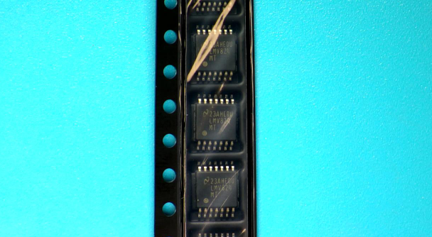
LMV824MTX/NOPB COUNTRY OF ORIGIN
|
LMV824MTX/NOPB PARAMETER INFORMATION
|
LMV824MTX/NOPB PACKAGING INFORMATION
|
LMV824MTX/NOPB MANUFACTURING INFORMATION
|
LMV824MTX/NOPB TYPE OF PACKAGING
|
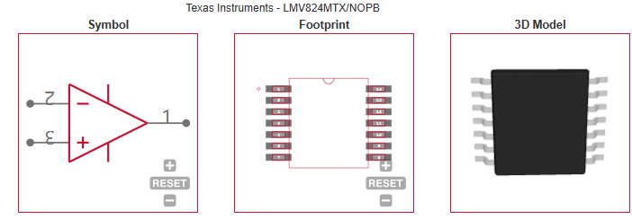
| LMV824MTX/NOPB ECAD MODELS |
LMV824MTX/NOPB APPLICATIONS
|
|
COUNTRY OF ORIGIN
|
Taiwan (Province of China)
|
Malaysia
|
|
PARAMETER INFORMATION
|
| Manufacturer Type |
Low Voltage Amplifier |
| type |
Low Voltage Amplifier |
| Rail to Rail |
Rail to Rail Output |
| Minimum Single Supply Voltage (V) |
2.5 |
| Number of Channels per Chip |
4 |
| Minimum PSRR (dB) |
75 |
| Typical Single Supply Voltage (V) |
2.7|5 |
| Maximum Single Supply Voltage (V) |
5.5 |
| Minimum Dual Supply Voltage (V) |
±1.25 |
| Typical Gain Bandwidth Product (MHz) |
5.6 |
| Maximum Input Offset Voltage (mV) |
3.5@5V |
| Maximum Input Offset Current (uA) |
0.03@5V |
| Maximum Dual Supply Voltage (V) |
±2.75 |
| Maximum Operating Supply Voltage (V) |
±2.75|5.5 |
| Maximum Input Bias Current (uA) |
0.1@5V |
| Minimum CMRR (dB) |
72 |
| Maximum Supply Voltage Range (V) |
5.5 to 6 |
| Minimum CMRR Range (dB) |
71 to 75 |
| Typical Voltage Gain (dB) |
105 |
| Typical Slew Rate (V/us) |
2@5V |
| Typical Input Offset Current (uA) |
0.0005@5V |
| Minimum Slew Rate (V/us) |
1.4@5V |
| Typical Output Current (mA) |
45@5V |
| Typical Input Noise Voltage Density (nV/rtHz) |
24@5V |
| Typical Noninverting Input Current Noise Density (pA/rtHz) |
0.25@5V |
| Typical Input Bias Current (uA) |
0.04@5V |
| Shut Down Support |
no |
| Minimum Operating Temperature (°C) |
-40 |
| Maximum Operating Temperature (°C) |
85 |
| Minimum Storage Temperature (°C) |
-65 |
| Maximum Storage Temperature (°C) |
150 |
| Power Supply Type |
Single|Dual |
| Maximum Supply Current (mA) |
1.3@5V |
| Input Offset Voltage Drift (uV/°C) |
1(Typ) |
|
|
PACKAGING INFORMATION
|
| Supplier Packaging |
TSSOP |
| Basic package types |
Lead-Frame SMT |
| Number of Pins |
14 |
| Pin shape |
Gull-wing |
| PCB |
14 |
| Ear piece |
N/R |
| Pin spacing (mm) |
0.65 |
| Package length (mm) |
5.1(Max) |
| Package width (mm) |
4.5(Max) |
| Package height (mm) |
1.05(Max) |
| Package diameter (mm) |
N/R |
| Package Overall Length (mm) |
5.1(Max) |
| Package Overall Width (mm) |
6.6(Max) |
| Package Overall Height (mm) |
1.2(Max) |
| Mounting surface height (mm) |
1.2(Max) |
| Install |
Surface Mount |
| Package weight (g) |
not applicable |
| Packaging materials |
Plastic |
| package instruction |
Thin Shrink Small Outline Package |
| Package Series Name |
SO |
| JEDEC |
MO-153AB-1 |
| Package Outline |
Link to data sheet |
|
|
MANUFACTURING INFORMATION
|
| MSL |
1 |
| Maximum reflow temperature (°C) |
260 |
| Reflow time (seconds) |
30 |
| Reflow cycles |
3 |
| standard |
J-STD-020D |
| Reflow temperature source |
Link to data sheet |
| Maximum wave soldering temperature (°C) |
N/R |
| Wave soldering time (seconds) |
N/R |
| Lead Finish(Plating) |
Matte Sn|Au |
| Plating materials |
N/A|Pd over Ni |
| Terminal base material |
Cu Alloy |
| Number of Wave Cycles |
N/R |
|
|
TYPE OF PACKAGING
|
| Packaging Suffix |
X |
| Package |
Tape and Reel Packaging |
| Packing quantity |
2500 |
| Reel Diameter (in) |
13 |
| Reel Width (mm) |
12.4 |
| Tape Pitch (mm) |
8 |
| Tape Width (mm) |
12 |
| Component Orientation |
Q1 |
| Package Type File |
Link to data sheet |
|
|
ECAD MODELS
|
|
|
APPLICATIONS
|
• Cordless Phones
|
• Cellular Phones
|
• Laptops
|
• PDAs
|
• PCMCIA
|
|