 |
||||||||||||||||||||||||||||||||||||||||
| |
||||||||||||||||||||||||||||||||||||||||
| • Integrated Shielded Inductor | ||||||||||||||||||||||||||||||||||||||||
| • Simple PCB Layout | ||||||||||||||||||||||||||||||||||||||||
| • Flexible Start-Up Sequencing Using External Soft-Start and Precision Enable | ||||||||||||||||||||||||||||||||||||||||
| • Protection Against Inrush Currents and FaultsSuch as Input UVLO and Output Short Circuit | ||||||||||||||||||||||||||||||||||||||||
| • Junction Temperature Range: –40°C to 125°C | ||||||||||||||||||||||||||||||||||||||||
| • Single Exposed Pad and Standard Pinout for Easy Mounting and Manufacturing | ||||||||||||||||||||||||||||||||||||||||
| • Fast Transient Response for Powering FPGAsand ASICs | ||||||||||||||||||||||||||||||||||||||||
| • Low Output Voltage Ripple | ||||||||||||||||||||||||||||||||||||||||
| • Pin-to-Pin Compatible Family: – LMZ14203/2/1 (42 V Maximum; 3 A, 2 A, 1 A) – LMZ12003/2/1 (20 V Maximum; 3 A, 2 A, 1 A) |
||||||||||||||||||||||||||||||||||||||||
| • Fully Enabled for WEBENCH® Power Designer | ||||||||||||||||||||||||||||||||||||||||
| • Electrical Specifications – 12-W Maximum Total Output Power – Up to 2-A Output Current – Input Voltage Range: 6 V to 42 V – Output Voltage Range: 0.8 V to 6 V – Efficiency up Ot 90% |
||||||||||||||||||||||||||||||||||||||||
| • Performance Benefits – Operates at High Ambient Temperature With No Thermal Derating – High Efficiency Reduces System Heat Generation – Low Radiated Emissions (EMI) Tested With EN55022 Class B Standard – Low External Component Count |
||||||||||||||||||||||||||||||||||||||||
| |
||||||||||||||||||||||||||||||||||||||||
| CATALOG | ||||||||||||||||||||||||||||||||||||||||
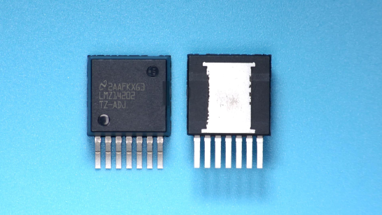
| LMZ14202TZE-ADJ/NOPB COUNTRY OF ORIGIN | ||||||||||||||||||||||||||||||||||||||||
| LMZ14202TZE-ADJ/NOPB PARAMETRIC INFO | ||||||||||||||||||||||||||||||||||||||||
| LMZ14202TZE-ADJ/NOPB PACKAGE INFO | ||||||||||||||||||||||||||||||||||||||||
| LMZ14202TZE-ADJ/NOPB MANUFACTURING INFO | ||||||||||||||||||||||||||||||||||||||||
| LMZ14202TZE-ADJ/NOPB PACKAGING INFO | ||||||||||||||||||||||||||||||||||||||||
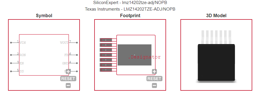
| LMZ14202TZE-ADJ/NOPB ECAD MODELS | ||||||||||||||||||||||||||||||||||||||||
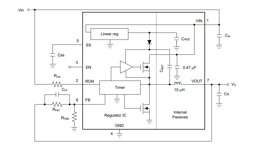
| LMZ14202TZE-ADJ/NOPB FUNCTIONAL BLOCK DIAGRAM | ||||||||||||||||||||||||||||||||||||||||
| LMZ14202TZE-ADJ/NOPB APPLICATIONS | ||||||||||||||||||||||||||||||||||||||||
| |
||||||||||||||||||||||||||||||||||||||||
| COUNTRY OF ORIGIN | ||||||||||||||||||||||||||||||||||||||||
| Malaysia | ||||||||||||||||||||||||||||||||||||||||
| |
||||||||||||||||||||||||||||||||||||||||
| PARAMETRIC INFO | ||||||||||||||||||||||||||||||||||||||||
|
||||||||||||||||||||||||||||||||||||||||
| PACKAGE INFO | ||||||||||||||||||||||||||||||||||||||||
|
||||||||||||||||||||||||||||||||||||||||
| MANUFACTURING INFO | ||||||||||||||||||||||||||||||||||||||||
|
||||||||||||||||||||||||||||||||||||||||
| PACKAGING INFO | ||||||||||||||||||||||||||||||||||||||||
|
||||||||||||||||||||||||||||||||||||||||
| ECAD MODELS | ||||||||||||||||||||||||||||||||||||||||
 |
||||||||||||||||||||||||||||||||||||||||
| FUNCTIONAL BLOCK DIAGRAM | ||||||||||||||||||||||||||||||||||||||||
 |
||||||||||||||||||||||||||||||||||||||||
| |
||||||||||||||||||||||||||||||||||||||||
| APPLICATIONS | ||||||||||||||||||||||||||||||||||||||||
| • Point of Load Conversions from 12-V and 24-V Input Rail | ||||||||||||||||||||||||||||||||||||||||
| • Time-Critical Projects | ||||||||||||||||||||||||||||||||||||||||
| • Space Constrained and High Thermal Requirement Applications Easy-To-Use, 7-Pin Package PFM 7-Pin Package | ||||||||||||||||||||||||||||||||||||||||
| • Negative Output Voltage Applications (See AN-2027) SNVA425 | ||||||||||||||||||||||||||||||||||||||||
| |