|
|
• Operating Input Voltage Range: 2.1 V to 16 V
|
• Ultralow-Dropout Voltage
|
• Output Voltage Accuracy 0.75% (A Grade)
|
• Specified 100-mA Output Current
|
• < 1-μA Quiescent Current when Shutdown
|
• Low Ground Pin Current at All Load Currents
|
• High Peak Current Capability (300 mA Typical)
|
• Wide Supply Voltage Range (16 V Maximum)
|
• Fast Dynamic Response to Line and Load
|
• Low ZOUT Over Wide Frequency Range
|
• Overtemperature and Overcurrent Protection
|
• −40°C to 125°C Junction Temperature Range
|
| |
| CATALOG |
|
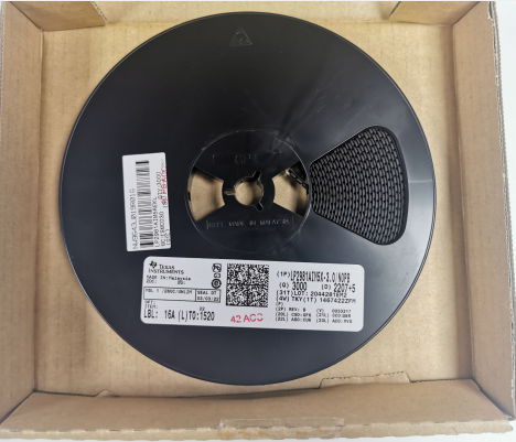
| LP2981AIM5X-3.0/NOPB COUNTRY OF ORIGIN |
LP2981AIM5X-3.0/NOPB PARAMETRIC INFO
|
LP2981AIM5X-3.0/NOPB PACKAGE INFO
|
LP2981AIM5X-3.0/NOPB MANUFACTURING INFO
|
LP2981AIM5X-3.0/NOPB PACKAGING INFO
|
LP2981AIM5X-3.0/NOPB ECAD MODELS
|
LP2981AIM5X-3.0/NOPB FUNCTIONAL BLOCK DIAGRAM
|
LP2981AIM5X-3.0/NOPB APPLICATIONS
|
|
COUNTRY OF ORIGIN
|
| USA |
| |
PARAMETRIC INFO
|
| Type |
LDO |
| Number of Outputs |
1 |
| Maximum Output Current (A) |
0.1 |
| Minimum Operating Temperature (°C) |
-40 |
| Maximum Operating Temperature (°C) |
125 |
| Output Type |
Fixed |
| Output Voltage Range (V) |
1.8 to 10 |
| Junction to Ambient |
220°C/W |
| Polarity |
Positive |
| Special Features |
Current Limit|Thermal Protection |
| Line Regulation |
0.014%/V |
| Maximum Dropout Voltage @ Current (V) |
0.003@0mA|0.01@1mA|0.1@25mA|0.25@100mA |
| Minimum Input Voltage (V) |
2.1 |
| Maximum Input Voltage (V) |
16 |
| Output Voltage (V) |
3 |
| Typical Quiescent Current (mA) |
0.065 |
| Typical Dropout Voltage @ Current (V) |
0.007@1mA|0.07@25mA|0.2@100mA |
| Accuracy (%) |
±1 |
| Minimum Storage Temperature (°C) |
-65 |
| Maximum Storage Temperature (°C) |
150 |
| Typical PSRR (dB) |
41 |
| Typical Output Capacitance (uF) |
2.2(Min) |
| Typical Output Noise Voltage (uVrms) |
160 |
|
| |
PACKAGE INFO
|
| Supplier Package |
SOT-23 |
| Basic Package Type |
Lead-Frame SMT |
| Pin Count |
5 |
| Lead Shape |
Gull-wing |
| PCB |
5 |
| Tab |
N/R |
| Pin Pitch (mm) |
0.95 |
| Package Length (mm) |
3.05(Max) |
| Package Width (mm) |
1.75(Max) |
| Package Height (mm) |
1.1 |
| Package Diameter (mm) |
N/R |
| Package Overall Length (mm) |
3.05(Max) |
| Package Overall Width (mm) |
3(Max) |
| Package Overall Height (mm) |
1.45(Max) |
| Seated Plane Height (mm) |
1.45(Max) |
| Mounting |
Surface Mount |
| Package Weight (g) |
N/A |
| Package Material |
Plastic |
| Package Description |
Small Outline Transistor |
| Package Family Name |
SOT |
| Jedec |
MO-178AA |
| Package Outline |
Link to Datasheet |
|
| |
Manufacturing Info
|
| MSL |
1 |
| Maximum Reflow Temperature (°C) |
260 |
| Reflow Solder Time (Sec) |
30 |
| Number of Reflow Cycle |
3 |
| Standard |
J-STD-020D |
| Reflow Temp. Source |
Link to Datasheet |
| Maximum Wave Temperature (°C) |
N/R |
| Wave Solder Time (Sec) |
N/R |
| Lead Finish(Plating) |
Matte Sn |
| Under Plating Material |
N/A |
| Terminal Base Material |
Cu Alloy |
|
| |
Packaging Info
|
| Packaging Suffix |
X |
| Packaging |
Tape and Reel |
| Quantity Of Packaging |
3000 |
| Reel Diameter (in) |
7 |
| Reel Width (mm) |
8.4 |
| Tape Pitch (mm) |
4 |
| Tape Width (mm) |
8 |
| Component Orientation |
Q3 |
| Packaging Document |
Link to Datasheet |
|
| |
ECAD MODELS
|

|
|
FUNCTIONAL BLOCK DIAGRAM
|
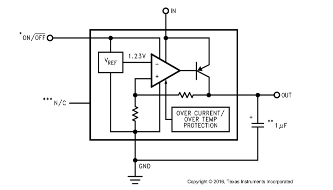
|
| |
APPLICATIONS
|
• Cellular Phones
|
• Palmtop and Laptop Computers
|
• Personal Digital Assistants (PDA)
|
• Camcorders, Personal Stereos, Cameras
|
|