|
|
• VIN range: 2.5 V to 16 V
|
• VOUT range (new chip):
– 1.2 V to 5.0 V (fixed, 100-mV steps)
|
• VOUT range (legacy chip): 2.5 V to 6.1 V
|
• VOUT accuracy:
– ±1% for A-grade legacy chip
– ±1.5% for standard-grade legacy chip
– ±0.5% for new chip only
|
• Output accuracy over load, and temperature:
– ±1% for new chip
|
| • Output current: Up to 150 mA |
| • Low IQ (new chip): 71 μA at ILOAD = 0 mA |
| • Low IQ (new chip): 750 μA at ILOAD = 150 mA |
| • Shutdown current:
– 0.05 μA (typ) for legacy chip
– 1.12 μA (typ) for new chip |
| • Low noise: 30 μVRMS with 10-nF bypass capacitor |
| • Output current limiting and thermal protection |
| • Stable with 2.2-µF ceramic capacitors |
| • High PSRR: 70 dB at 1 kHz, 40 dB at 1 MHz |
| • Operating junction temperature: –40°C to +125°C |
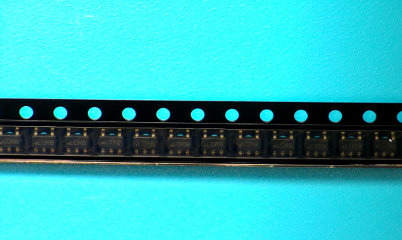
| • Package: 5-pin SOT-23 (DBV) ultra-low dropout
voltage |
|
| CATALOG |
LP2985IM5X-3.3/NOPB COUNTRY OF ORIGIN
|
LP2985IM5X-3.3/NOPB PARAMETRIC INFO
|
LP2985IM5X-3.3/NOPB PACKAGE INFO
|
LP2985IM5X-3.3/NOPB MANUFACTURING INFO
|
LP2985IM5X-3.3/NOPB PACKAGING INFO
|
LP2985IM5X-3.3/NOPB ECAD MODELS
|
LP2985IM5X-3.3/NOPB APPLICATIONS
|
|
COUNTRY OF ORIGIN
|
| China |
| Thailand |
| Philippines |
| Malaysia |
|
PARAMETRIC INFO
|
| Type |
LDO |
| Number of Outputs |
1 |
| Maximum Output Current (A) |
0.15 |
| Minimum Operating Temperature (°C) |
-40 |
| Maximum Operating Temperature (°C) |
125 |
| Output Type |
Fixed |
| Output Voltage Range (V) |
1.8 to 10 |
| Junction to Ambient |
169°C/W |
| Junction to Case |
121.8°C/W |
| Polarity |
Positive |
| Special Features |
Current Limit|Thermal Protection |
| Line Regulation |
0.014%/V |
| Maximum Dropout Voltage @ Current (V) |
0.003@0mA|0.01@1mA|0.06@10mA|0.15@50mA|0.35@150mA |
| Minimum Input Voltage (V) |
2.5 |
| Maximum Input Voltage (V) |
16 |
| Output Voltage (V) |
3.3 |
| Typical Quiescent Current (mA) |
0.065 |
| Typical Dropout Voltage @ Current (V) |
0.0001@0mA|0.007@1mA|0.04@10mA|0.12@50mA|0.28@150mA |
| Accuracy (%) |
±3 |
| Minimum Storage Temperature (°C) |
-65 |
| Maximum Storage Temperature (°C) |
150 |
| Typical PSRR (dB) |
45 |
| Typical Output Noise Voltage (uVrms) |
30 |
| Output Capacitor Type |
Ceramic |
|
|
PACKAGE INFO
|
| Supplier Package |
SOT-23 |
| Basic Package Type |
Lead-Frame SMT |
| Pin Count |
5 |
| Lead Shape |
Gull-wing |
| PCB |
5 |
| Tab |
N/R |
| Pin Pitch (mm) |
0.95 |
| Package Length (mm) |
3.05(Max) |
| Package Width (mm) |
1.75(Max) |
| Package Height (mm) |
1.1 |
| Package Diameter (mm) |
N/R |
| Package Overall Length (mm) |
3.05(Max) |
| Package Overall Width (mm) |
3(Max) |
| Package Overall Height (mm) |
1.45(Max) |
| Seated Plane Height (mm) |
1.45(Max) |
| Mounting |
Surface Mount |
| Package Weight (g) |
N/A |
| Package Material |
Plastic |
| Package Description |
Small Outline Transistor |
| Package Family Name |
SOT |
| Jedec |
MO-178 |
|
|
MANUFACTURING INFO
|
| MSL |
1 |
| Maximum Reflow Temperature (°C) |
260 |
| Reflow Solder Time (Sec) |
30 |
| Number of Reflow Cycle |
3 |
| Standard |
J-STD-020D |
| Reflow Temp. Source |
Link to Datasheet |
| Maximum Wave Temperature (°C) |
260 |
| Wave Solder Time (Sec) |
4 |
| Wave Temp. Source |
Link to Datasheet |
| Lead Finish(Plating) |
Matte Sn|Au |
| Under Plating Material |
N/A|Pd over Ni |
| Terminal Base Material |
Cu Alloy|N/A |
| Number of Wave Cycles |
N/A |
|
|
PACKAGING INFO
|
| Packaging Suffix |
X |
| Packaging |
Tape and Reel |
| Quantity Of Packaging |
3000 |
| Reel Diameter (in) |
7 |
| Reel Width (mm) |
8.4 |
| Tape Pitch (mm) |
4 |
| Tape Width (mm) |
8 |
| Component Orientation |
Q3 |
| Packaging Document |
Link to Datasheet |
|
|
ECAD MODELS
|
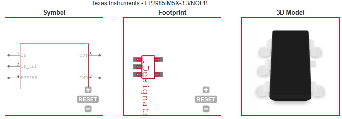
|
|
APPLICATIONS
|
• Washers and dryers
|
| • Land mobile radios |
• Active antenna system mMIMO
|
• Cordless power tools
|
• Motor drives and control boards
|
| |
| |