|
|
• Input Supply Voltage: 2.5 V to 16V
|
• Output Voltage Range: 1 V to 5.5 V
|
• Very Low Output Noise
|
• < 10-μA Quiescent Current in Shutdown
|
• Low Ground Pin Current at all Loads
|
• Overtemperature and Overcurrent Protection
|
|
| CATALOG |
LP3878SD-ADJ/NOPB COUNTRY OF ORIGIN
|
LP3878SD-ADJ/NOPB PARAMETRIC INFO
|
LP3878SD-ADJ/NOPB PACKAGE INFO
|
LP3878SD-ADJ/NOPB MANUFACTURING INFO
|
LP3878SD-ADJ/NOPB PACKAGING INFO
|
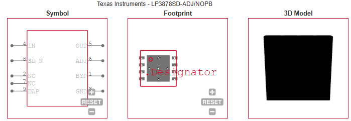
LP3878SD-ADJ/NOPB ECAD MODELS
|
LP3878SD-ADJ/NOPB APPLICATIONS
|
|
COUNTRY OF ORIGIN
|
Thailand
|
Malaysia
|
|
PARAMETRIC INFO
|
| Type |
LDO |
| Number of Outputs |
1 |
| Maximum Output Current (A) |
0.8 |
| Minimum Operating Temperature (°C) |
-40 |
| Maximum Operating Temperature (°C) |
125 |
| Regulation Condition Change In Line |
13V |
| Output Type |
Adjustable |
| Output Voltage Range (V) |
<1.8|1.8 to 10 |
| Junction to Ambient |
38.1°C/W |
| Junction to Case |
27.9°C/W |
| Polarity |
Positive |
| Special Features |
Current Limit|Thermal Protection |
| Line Regulation |
0.01%/V(Typ) |
| Maximum Dropout Voltage @ Current (V) |
0.002@100uA|0.2@200mA|0.6@800mA |
| Minimum Input Voltage (V) |
2.5 |
| Maximum Input Voltage (V) |
16 |
| Output Voltage (V) |
1 to 5.5 |
| Typical Quiescent Current (mA) |
5.5 |
| Typical Dropout Voltage @ Current (V) |
0.001@100uA|0.15@200mA|0.475@800mA |
| Accuracy (%) |
±1 |
| Minimum Storage Temperature (°C) |
-65 |
| Maximum Storage Temperature (°C) |
150 |
| Typical Ground Current @ Full Load (mA) |
5.5 |
| Typical PSRR (dB) |
60 |
| Typical Output Noise Voltage (uVrms) |
18 |
| Output Capacitor Type |
Ceramic |
|
|
PACKAGE INFO
|
| Supplier Package |
WSON EP |
| Basic Package Type |
Non-Lead-Frame SMT |
| Pin Count |
8 |
| Lead Shape |
No Lead |
| PCB |
8 |
| Tab |
N/R |
| Pin Pitch (mm) |
0.8 |
| Package Length (mm) |
4.1(Max) |
| Package Width (mm) |
4.1(Max) |
| Package Height (mm) |
0.75(Max) |
| Package Diameter (mm) |
N/R |
| Package Overall Length (mm) |
4.1(Max) |
| Package Overall Width (mm) |
4.1(Max) |
| Package Overall Height (mm) |
0.8(Max) |
| Seated Plane Height (mm) |
0.8(Max) |
| Mounting |
Surface Mount |
| Package Weight (g) |
N/A |
| Package Material |
Plastic |
| Package Description |
Very Very Thin Small Outline No Lead Package, Exposed Pad |
| Package Family Name |
SON |
| Jedec |
N/A |
| Package Outline |
Link to Datasheet |
|
|
MANUFACTURING INFO
|
| MSL |
1 |
| Maximum Reflow Temperature (°C) |
260 |
| Reflow Solder Time (Sec) |
30 |
| Number of Reflow Cycle |
3 |
| Standard |
J-STD-020D |
| Reflow Temp. Source |
Link to Datasheet |
| Maximum Wave Temperature (°C) |
N/R |
| Wave Solder Time (Sec) |
N/R |
| Lead Finish(Plating) |
Matte Sn|Au |
| Under Plating Material |
N/A|Pd over Ni |
| Terminal Base Material |
Cu Alloy|N/A |
| Number of Wave Cycles |
N/R |
|
|
PACKAGING INFO
|
| Packaging |
Tape and Reel |
| Quantity Of Packaging |
1000 |
| Reel Diameter (in) |
7.09 |
| Reel Width (mm) |
12.4 |
| Tape Pitch (mm) |
8 |
| Tape Width (mm) |
12 |
| Component Orientation |
Q1 |
| Packaging Document |
Link to Datasheet |
|
|
ECAD MODELS
|
|
|
APPLICATIONS
|
• DSP and FPGA Power Supplies
|
| • SMPS Post-Regulator |
| • Medical Instrumentation |
|