 |
|
| • Wide Operating Input Voltage Range:
3 V to 20 V |
| • Ultra-Low Output Noise: 5 µVRMS
(10 Hz to 100 kHz) |
| • High PSRR: 90 dB at 10 kHz, 60 dB at 100 kHz |
| • ±1% Output Voltage Initial Accuracy (TJ = 25°C) |
| • Very Low Dropout: 200 mV (Typical) at 800 mA |
| • Stable with Ceramic or Tantalum Output
Capacitors |
| • Excellent Line and Load Transient Response |
| • Current Limit and Overtemperature Protection |
| • Create a Custom Design Using the LP38798 With
the WEBENCH® Power Designer |
|
| CATALOG |
| LP38798SDE-ADJ/NOPB COUNTRY OF ORIGIN |
| LP38798SDE-ADJ/NOPB PARAMETRIC INFO |
| LP38798SDE-ADJ/NOPB PACKAGE INFO |
| LP38798SDE-ADJ/NOPB MANUFACTURING INFO |
| LP38798SDE-ADJ/NOPB PACKAGING INFO |
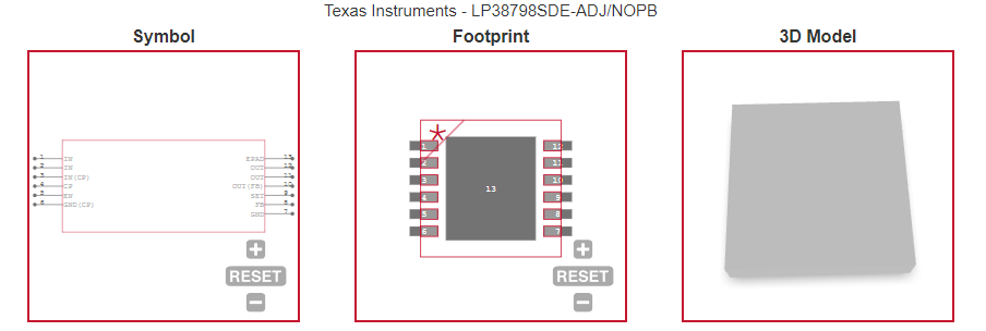
| LP38798SDE-ADJ/NOPB ECAD MODELS |
| LP38798SDE-ADJ/NOPB FUNCTIONAL BLOCK DIAGRAM |
| LP38798SDE-ADJ/NOPB APPLICATIONS |
|
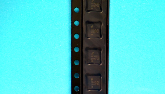
| COUNTRY OF ORIGIN |
| Malaysia |
|
| PARAMETRIC INFO |
| Type |
LDO |
| Number of Outputs |
1 |
| Maximum Output Current (A) |
0.8 |
| Minimum Operating Temperature (°C) |
-40 |
| Maximum Operating Temperature (°C) |
125 |
| Output Type |
Adjustable |
| Output Voltage Range (V) |
<1.8|1.8 to 10|10 to 20 |
| Regulation Condition Change In Load |
790mA |
| Regulation Condition Change In Line |
14.5V |
| Junction to Ambient |
138°C/W |
| Junction to Case |
5°C/W |
| Polarity |
Positive |
| Special Features |
Current Limit|Thermal Protection |
| Process Technology |
CMOS |
| Line Regulation |
0.005%/V(Typ) |
| Maximum Quiescent Current (mA) |
2.1 |
| Maximum Dropout Voltage @ Current (V) |
0.42@800mA |
| Minimum Input Voltage (V) |
3 |
| Maximum Input Voltage (V) |
20 |
| Output Voltage (V) |
1.2 to 19.8 |
| Typical Quiescent Current (mA) |
1.4 |
| Typical Dropout Voltage @ Current (V) |
0.2@800mA |
| Reference Voltage (V) |
1.212 |
| Accuracy (%) |
±1 |
| Minimum Storage Temperature (°C) |
-65 |
| Maximum Storage Temperature (°C) |
150 |
| Typical Ground Current @ Full Load (mA) |
1.6 |
| Typical PSRR (dB) |
110 |
| Typical Output Capacitance (uF) |
1 |
| Typical Output Noise Voltage (uVrms) |
11.58 |
| Pass Element Type |
NMOS |
| Output Capacitor Type |
Ceramic|Tantalum |
|
| |
| PACKAGE INFO |
| Supplier Package |
WSON EP |
| Basic Package Type |
Non-Lead-Frame SMT |
| Pin Count |
12 |
| Lead Shape |
No Lead |
| PCB |
12 |
| Tab |
N/R |
| Pin Pitch (mm) |
0.5 |
| Package Length (mm) |
4.1(Max) |
| Package Width (mm) |
4.1(Max) |
| Package Height (mm) |
0.75(Max) |
| Package Diameter (mm) |
N/R |
| Package Overall Length (mm) |
4.1(Max) |
| Package Overall Width (mm) |
4.1(Max) |
| Package Overall Height (mm) |
0.8(Max) |
| Seated Plane Height (mm) |
0.8(Max) |
| Mounting |
Surface Mount |
| Package Weight (g) |
N/A |
| Package Material |
Plastic |
| Package Description |
Very Very Thin Small Outline No Lead Package, Exposed Pad |
| Package Family Name |
SON |
| Jedec |
N/A |
|
| |
| MANUFACTURING INFO |
| MSL |
1 |
| Maximum Reflow Temperature (°C) |
260 |
| Reflow Solder Time (Sec) |
30 |
| Number of Reflow Cycle |
3 |
| Standard |
J-STD-020D |
| Reflow Temp. Source |
Link to Datasheet |
| Maximum Wave Temperature (°C) |
N/R |
| Wave Solder Time (Sec) |
N/R |
| Lead Finish(Plating) |
Matte Sn |
| Under Plating Material |
N/A |
| Terminal Base Material |
Cu Alloy |
| Number of Wave Cycles |
N/R |
|
| |
| PACKAGING INFO |
| Packaging Suffix |
E |
| Packaging |
Tape and Reel |
| Quantity Of Packaging |
250 |
| Reel Diameter (in) |
7 |
| Reel Width (mm) |
12.4 |
| Tape Pitch (mm) |
8 |
| Tape Width (mm) |
12 |
| Component Orientation |
Q1 |
| Packaging Document |
Link to Datasheet |
|
| |
| ECAD MODELS |
 |
|
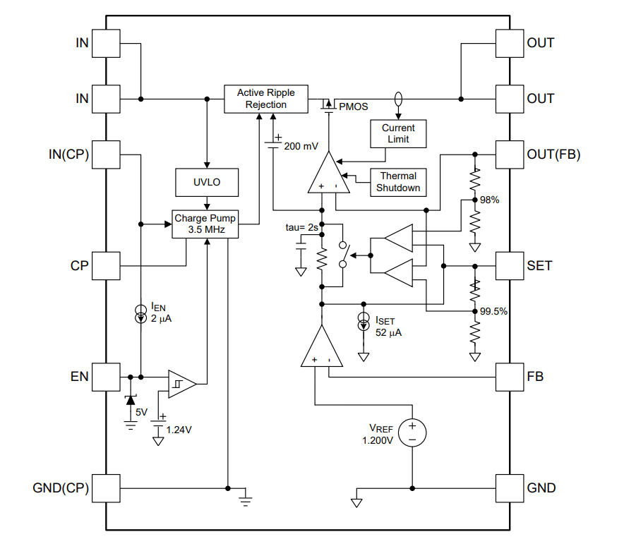
| FUNCTIONAL BLOCK DIAGRAM |
 |
|
| APPLICATIONS |
| • RF Power Supplies: PLLs, VCOs, Mixers, LNAs |
| • Telecom Infrastructure |
| • Wireless Infrastructure |
| • Very Low-Noise Instrumentation |
| • Precision Power Supplies |
| • High-Speed, High-Precision Data Converters |
|