|
|
• 12MHz Gain Bandwidth
|
• 400V/µs Slew Rate
|
• 1.25mA Maximum Supply Current per Amplifier
|
| • Unity-Gain Stable
|
| • C-Load™ Op Amp Drives All Capacitive Loads |
| • 10nV/√Hz Input Noise Voltage |
| • 800µV Maximum Input Offset Voltage |
| • 300nA Maximum Input Bias Current |
| • 70nA Maximum Input Offset Current |
| • 12V/mV Minimum DC Gain, RL = 1k |
| • 230ns Settling Time to 0.1%, 10V Step |
| • 280ns Settling Time to 0.01%, 10V Step |
| • ±12V Minimum Output Swing into 500Ω |
| • ±2.75V Minimum Output Swing into 150Ω |
| • Specified at ±2.5V, ±5V, and ±15V |
|
| CATALOG |
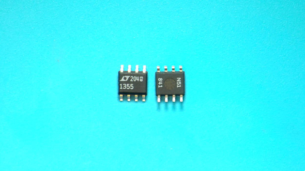
| LT1355CS8#PBF COUNTRY OF ORIGIN |
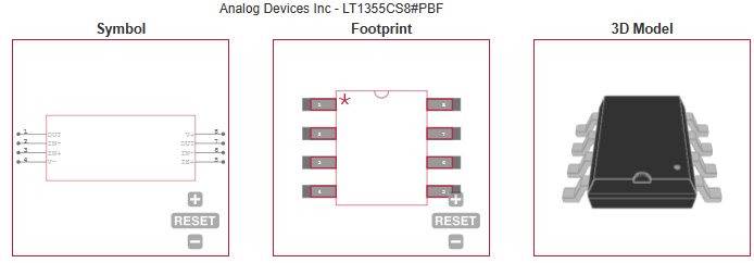
LT1355CS8#PBF PARAMETRIC INFO
|
LT1355CS8#PBF PACKAGE INFO
|
LT1355CS8#PBF MANUFACTURING INFO
|
LT1355CS8#PBF PACKAGING INFO
|
LT1355CS8#PBF EACD MODELS
|
| LT1355CS8#PBF APPLICATIONS |
|
| COUNTRY OF ORIGIN |
| Malaysia |
|
PARAMETRIC INFO
|
| Manufacturer Type |
High Speed Amplifier |
| type |
High Speed Amplifier |
| Number of Channels per Chip |
2 |
| Process Technology |
BiCOM |
| Minimum PSRR (dB) |
92 |
| Minimum Dual Supply Voltage (V) |
±2.5 |
| Typical Gain Bandwidth Product (MHz) |
10.5 |
| Maximum Input Offset Voltage (mV) |
0.8@±5V |
| Typical Dual Supply Voltage (V) |
±3|±5|±9|±12|±15 |
| Maximum Input Offset Current (uA) |
0.07@±15V |
| Maximum Dual Supply Voltage (V) |
±18 |
| Maximum Operating Supply Voltage (V) |
±18 |
| Maximum Input Bias Current (uA) |
0.3@±15V |
| Minimum CMRR (dB) |
78 |
| Maximum Supply Voltage Range (V) |
36 to 37 |
| Minimum CMRR Range (dB) |
75 to 80 |
| Typical Voltage Gain (dB) |
91.13 |
| Typical Slew Rate (V/us) |
120@±5V |
| Typical Settling Time (ns) |
380 |
| Typical Output Current (mA) |
25@±5V |
| Typical Input Noise Voltage Density (nV/rtHz) |
10@±15V |
| Typical Noninverting Input Current Noise Density (pA/rtHz) |
0.6@±15V |
| Shut Down Support |
no |
| Minimum Operating Temperature (°C) |
0 |
| Maximum Operating Temperature (°C) |
70 |
| Supplier Temperature Rating |
Commercial |
| Power Supply Type |
Dual |
| Maximum Supply Current (mA) |
2.4@±5V |
|
|
PACKAGE INFO
|
| Supplier packaging |
SOIC N |
| Basic package type |
Lead-Frame SMT |
| Number of pins |
8 |
| Pin shape |
Gull-wing |
| PCB |
8 |
| ears |
N/R |
| Pin spacing (mm) |
1.27 |
| Package length (mm) |
5(Max) |
| Package width (mm) |
3.99(Max) |
| Package height (mm) |
1.5(Max) |
| Package diameter (mm) |
N/R |
| Package Overall Length (mm) |
5(Max) |
| Package Overall Width (mm) |
6.2(Max) |
| Package Overall Height (mm) |
1.75(Max) |
| Mounting surface height (mm) |
1.75(Max) |
| Install |
Surface Mount |
| Package weight (g) |
not applicable |
| Packaging materials |
Plastic |
| package instruction |
Small Outline IC Narrow Body |
| Package series name |
SO |
| JEDEC |
MS-012AA |
| Package outline |
Link to datasheet |
|
|
MANUFACTURING INFO
|
| MSL |
1 |
| Maximum reflow temperature (°C) |
260 |
| Reflow soldering time (seconds) |
30 |
| Number of reflow cycles |
3 |
| standard |
J-STD-020D |
| Reflow temperature source |
Link to datasheet |
| Maximum wave soldering temperature (°C) |
260 |
| Wave soldering time (seconds) |
10 |
| Wave soldering temperature source |
Link to datasheet |
| Lead Finish(Plating) |
Matte Sn annealed |
| Plating materials |
Ag |
| Terminal Base Material |
Alloy 42 |
| Number of Wave Cycles |
not applicable |
|
|
PACKAGING INFO
|
| Package |
Tube |
| Packing quantity |
100 |
|
|
ECAD MODELS
|
|
|
| APPLICATIONS |
| • Wideband Amplifiers |
| • Buffers |
| • Active Filters |
| • Data Acquisition Systems |
| • Photodiode Amplifiers |
| |