 |
|
| ■ Optimized for Fast Transient Response |
| ■ Output Current: 3A |
| ■ Dropout Voltage: 340mV at 3A |
| ■ Low Noise: 40µVRMS (10Hz to 100kHz) |
| ■ 1mA Quiescent Current |
| ■ Wide Input Voltage Range: 2.7V to 20V |
| ■ No Protection Diodes Needed |
| ■ Controlled Quiescent Current in Dropout |
| ■ Fixed Output Voltages: 1.5V, 1.8V, 2.5V, 3.3V |
| ■ Adjustable Output from 1.21V to 20V |
| ■ <1µA Quiescent Current in Shutdown |
| ■ Stable with 10µF Output Capacitor |
| ■ Reverse Battery Protection |
| ■ No Reverse Current |
| ■ Thermal Limiting |
| ■ Available in 5-Lead TO-220, DD and 16-Lead
TSSOP Packages |
|
| CATALOG |
| LT1764EQ#TRPBF COUNTRY OF ORIGIN |
| LT1764EQ#TRPBF PARAMETRIC INFO |
| LT1764EQ#TRPBF PACKAGE INFO |
| LT1764EQ#TRPBF MANUFACTURING INFO |
| LT1764EQ#TRPBF PACKAGING INFO |
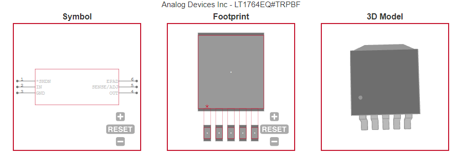
| LT1764EQ#TRPBF ECAD MODELS |
| LT1764EQ#TRPBF APPLICATIOS |
|
| COUNTRY OF ORIGIN |
| Malaysia |
| United States of America |
|
| PARAMETRIC INFO |
| Type |
LDO |
| Number of Outputs |
1 |
| Maximum Output Current (A) |
3 |
| Minimum Operating Temperature (°C) |
-40 |
| Maximum Operating Temperature (°C) |
125 |
| Output Type |
Adjustable |
| Output Voltage Range (V) |
<1.8|1.8 to 10|10 to 20|20 to 50 |
| Regulation Condition Change In Load |
2.999A |
| Regulation Condition Change In Line |
17.79V |
| Junction to Ambient |
30°C/W |
| Polarity |
Positive |
| Special Features |
Current Limit|Reverse Battery Protection|Reverse Current Protection|Shutdown|Thermal Protection |
| Load Regulation |
5mV |
| Line Regulation |
10mV |
| Maximum Dropout Voltage @ Current (V) |
0.05@1mA|0.13@100mA|0.2@500mA|0.33@1.5A|0.45@3A|0.66@2700mA |
| Minimum Input Voltage (V) |
2.7 |
| Maximum Input Voltage (V) |
20 |
| Output Voltage (V) |
1.21 to 20 |
| Typical Quiescent Current (mA) |
1 |
| Typical Dropout Voltage @ Current (V) |
0.02@1mA|0.07@100mA|0.14@500mA|0.25@1.5A|0.34@3A |
| Reference Voltage (V) |
1.21 |
| Accuracy (%) |
±1.5(Typ) |
| Supplier Temperature Grade |
Extended |
| Minimum Storage Temperature (°C) |
-65 |
| Maximum Storage Temperature (°C) |
150 |
| Typical Ground Current @ Full Load (mA) |
120 |
| Typical PSRR (dB) |
63 |
| Typical Output Capacitance (uF) |
10(Min) |
| Typical Output Noise Voltage (uVrms) |
40 |
| Output Capacitor Type |
Ceramic |
|
| |
| PACKAGE INFO |
| Supplier Package |
DDPAK |
| Basic Package Type |
Lead-Frame SMT |
| Pin Count |
6 |
| Lead Shape |
Gull-wing |
| PCB |
5 |
| Tab |
Tab |
| Pin Pitch (mm) |
1.7 |
| Package Length (mm) |
10.54(Max) |
| Package Width (mm) |
9.4(Max) |
| Package Height (mm) |
4.57(Max) |
| Package Diameter (mm) |
N/R |
| Package Overall Length (mm) |
10.54(Max) |
| Package Overall Width (mm) |
13.34(Max) |
| Package Overall Height (mm) |
4.88(Max) |
| Seated Plane Height (mm) |
4.88(Max) |
| Mounting |
Surface Mount |
| Package Weight (g) |
N/A |
| Package Material |
Plastic |
| Package Description |
Double Deca Watt Package |
| Package Family Name |
TO-263 |
| Jedec |
TO-263BA |
| Package Outline |
Link to Datasheet |
|
| |
| MANUFACTURING INFO |
| MSL |
1 |
| Maximum Reflow Temperature (°C) |
245 |
| Reflow Solder Time (Sec) |
30 |
| Number of Reflow Cycle |
3 |
| Standard |
J-STD-020D |
| Reflow Temp. Source |
Link to Datasheet |
| Maximum Wave Temperature (°C) |
260 |
| Wave Solder Time (Sec) |
10 |
| Wave Temp. Source |
Link to Datasheet |
| Lead Finish(Plating) |
Matte Sn annealed |
| Under Plating Material |
AgNi |
| Terminal Base Material |
Cu Alloy |
| Number of Wave Cycles |
2 |
|
| |
| PACKAGING INFO |
| Packaging Suffix |
TR |
| Packaging |
Tape and Reel |
| Quantity Of Packaging |
750 |
| Reel Diameter (in) |
13 |
| Reel Width (mm) |
24.4 |
| Tape Pitch (mm) |
16 |
| Tape Width (mm) |
24 |
| Feed Hole Pitch (mm) |
4 |
| Hole Center to Component Center (mm) |
2 |
| Component Orientation |
Tab Opposing Sprocket Hole |
| Packaging Document |
Link to Datasheet |
| Tape Type |
Embossed |
|
| |
| ECAD MODELS |
 |
|
| APPLICATIOS |
| ■ 3.3V to 2.5V Logic Power Supply |
| ■ Post Regulator for Switching Supplies |
|