|
|
• Wide Input Voltage Range: 3V to 80V
|
• Low Quiescent Current: 7µA
|
• Low Dropout Voltage: 350mV
|
• Output Current: 20mA
|
• LT3014HV Survives 100V Transients (2ms)
|
• No Protection Diodes Needed
|
• Adjustable Output from 1.22V to 60V
|
• 1µA Quiescent Current in Shutdown
|
|
| CATALOG |
LT3014ES5#TRMPBF COUNTRY OF ORIGIN
|
LT3014ES5#TRMPBF PARAMETRIC INFO
|
LT3014ES5#TRMPBF PACKAGE INFO
|
LT3014ES5#TRMPBF MANUFACTURING INFO
|
LT3014ES5#TRMPBF PACKAGING INFO
|
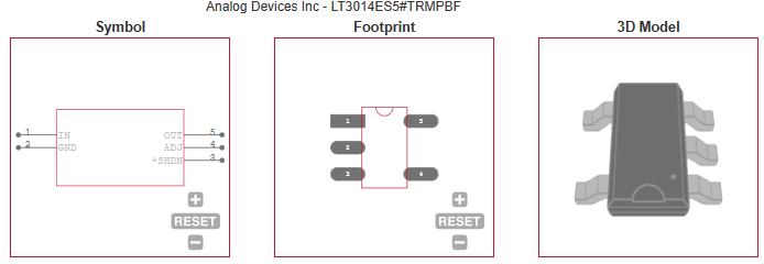
LT3014ES5#TRMPBF ECAD MODELS
|
LT3014ES5#TRMPBF APPLICATIONS
|
|
COUNTRY OF ORIGIN
|
United States of America
|
|
PARAMETRIC INFO
|
| Type |
LDO |
| Number of Outputs |
1 |
| Maximum Output Current (A) |
0.02 |
| Minimum Operating Temperature (°C) |
-40 |
| Maximum Operating Temperature (°C) |
125 |
| Output Voltage Range (V) |
<1.8|1.8 to 10|10 to 20|20 to 50|>=50 |
| Output Type |
Adjustable |
| Junction to Ambient |
150°C/W |
| Junction to Case |
25°C/W |
| Polarity |
Positive |
| Special Features |
Current Limit|Reverse Battery Protection|Reverse Current Protection|Shutdown|Thermal Protection |
| Load Regulation |
25mV |
| Line Regulation |
10mV |
| Maximum Dropout Voltage @ Current (V) |
0.18@100uA|0.27@1mA|0.35@10mA|0.41@20mA |
| Minimum Input Voltage (V) |
3 |
| Maximum Input Voltage (V) |
80 |
| Output Voltage (V) |
1.22 to 60 |
| Typical Quiescent Current (mA) |
0.007 |
| Typical Dropout Voltage @ Current (V) |
0.12@100uA|0.2@1mA|0.3@10mA|0.35@20mA |
| Reference Voltage (V) |
1.22 |
| Supplier Temperature Grade |
Extended |
| Typical PSRR (dB) |
70 |
| Typical Output Capacitance (uF) |
0.47 |
| Typical Output Noise Voltage (uVrms) |
115 |
| Output Capacitor Type |
Ceramic|Tantalum |
|
|
PACKAGE INFO
|
| Supplier Package |
TSOT-23 |
| Basic Package Type |
Lead-Frame SMT |
| Pin Count |
5 |
| Lead Shape |
Gull-wing |
| PCB |
5 |
| Tab |
N/R |
| Pin Pitch (mm) |
0.95 |
| Package Length (mm) |
2.9 |
| Package Width (mm) |
1.75(Max) |
| Package Height (mm) |
0.9(Max) |
| Package Diameter (mm) |
N/R |
| Package Overall Length (mm) |
2.9 |
| Package Overall Width (mm) |
2.8 |
| Package Overall Height (mm) |
1(Max) |
| Seated Plane Height (mm) |
1(Max) |
| Mounting |
Surface Mount |
| Package Weight (g) |
N/A |
| Package Material |
Plastic |
| Package Description |
Thin Small Outline Transistor |
| Package Family Name |
SOT |
| Jedec |
MO-193AB |
| Package Outline |
Link to Datasheet |
|
|
MANUFACTURING INFO
|
| MSL |
1 |
| Maximum Reflow Temperature (°C) |
260 |
| Reflow Solder Time (Sec) |
30 |
| Number of Reflow Cycle |
3 |
| Standard |
J-STD-020D |
| Reflow Temp. Source |
Link to Datasheet |
| Maximum Wave Temperature (°C) |
260 |
| Wave Solder Time (Sec) |
10 |
| Wave Temp. Source |
Link to Datasheet |
| Lead Finish(Plating) |
Matte Sn annealed |
| Under Plating Material |
Ag |
| Terminal Base Material |
Cu Alloy |
|
|
PACKAGING INFO
|
| Packaging Suffix |
TRM |
| Packaging |
Tape and Reel |
| Quantity Of Packaging |
500 |
| Reel Diameter (in) |
7 |
| Reel Width (mm) |
8.4 |
| Tape Pitch (mm) |
4 |
| Tape Width (mm) |
8 |
| Feed Hole Pitch (mm) |
4 |
| Hole Center to Component Center (mm) |
2 |
| Component Orientation |
3 Pin At Sprocket Hole |
| Packaging Document |
Link to Datasheet |
|
|
ECAD MODELS
|
|
|
APPLICATIONS
|
• Low Current High Voltage Regulators
|
• Regulator for Battery-Powered Systems
|
• Telecom Applications
|
• Automotive Applications
|
| |