|
|
• Ultralow RMS Noise: 0.8µVRMS (10Hz to 100kHz)
|
• Ultralow Spot Noise: 2nV/√Hz at 10kHz
|
• Ultrahigh PSRR: 79dB at 1MHz
|
• Output Current: 200mA
|
• Wide Input Voltage Range: 1.8V to 20V
|
• Single Capacitor Improves Noise and PSRR
|
• 100µA SET Pin Current: ±1% Initial Accuracy
|
• Single Resistor Programs Output Voltage
|
• High Bandwidth: 1MHz
|
• Programmable Current Limit
|
• Low Dropout Voltage: 350mV
|
• Output Voltage Range: 0V to 15V
|
• Programmable Power Good
|
• Fast Start-Up Capability
|
• Precision Enable/UVLO
|
• Parallelable for Lower Noise and Higher Current
|
• Internal Current Limit with Foldback
|
• Minimum Output Capacitor: 4.7µF Ceramic
|
• Reverse Battery and Reverse Current Protection
|
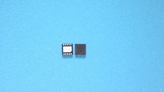
• 10-Lead MSOP and 3mm × 3mm DFN Packages
|
• AEC-Q100 Qualified for Automotive Applications
|
|
| CATALOG |
LT3042EDD#PBF COUNTRY OF ORIGIN
|
LT3042EDD#PBF PARAMETRIC INFO
|
LT3042EDD#PBF PACKAGE INFO
|
LT3042EDD#PBF MANUFACTURING INFO
|
LT3042EDD#PBF PACKAGING INFO
|
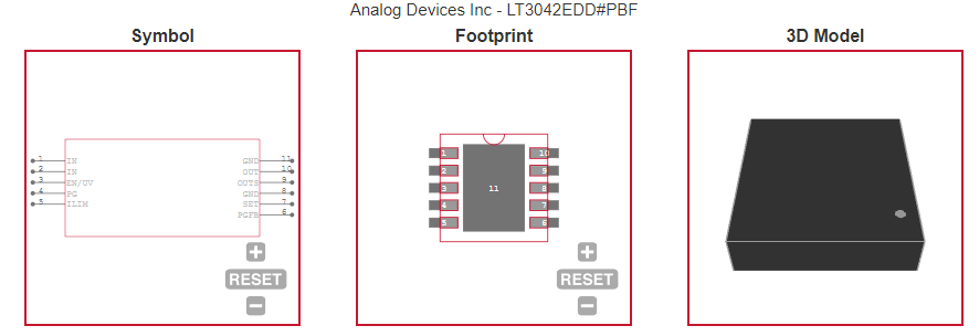
LT3042EDD#PBF ECAD MODELS
|
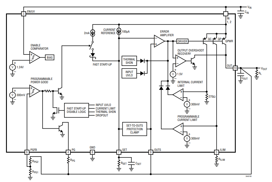
LT3042EDD#PBF FUNCTIONAL BLOCK DIAGRAM
|
LT3042EDD#PBF APPLICATIONS
|
|
COUNTRY OF ORIGIN
|
Thailand
|
Malaysia
|
Korea (Republic of)
|
Philippines
|
|
PARAMETRIC INFO
|
| Type |
LDO |
| Number of Outputs |
1 |
| Maximum Output Current (A) |
0.2 |
| Minimum Operating Temperature (°C) |
-40 |
| Maximum Operating Temperature (°C) |
125 |
| Output Type |
Adjustable |
| Output Voltage Range (V) |
<1.8|1.8 to 10|10 to 20 |
| Regulation Condition Change In Load |
199mA |
| Regulation Condition Change In Line |
18V |
| Junction to Ambient |
34°C/W |
| Junction to Case |
5.5°C/W |
| Polarity |
Positive |
| Special Features |
Reverse Battery Protection|Reverse Current Protection |
| Load Regulation |
3nA(Typ) |
| Line Regulation |
3uV/V |
| Maximum Dropout Voltage @ Current (V) |
0.27@1mA|0.27@50mA |
| Minimum Input Voltage (V) |
1.8 |
| Maximum Input Voltage (V) |
20 |
| Output Voltage (V) |
0 to 15 |
| Typical Quiescent Current (mA) |
2 |
| Typical Dropout Voltage @ Current (V) |
0.22@1mA|0.22@50mA|0.27@150mA|0.35@200mA |
| Accuracy (%) |
±1 |
| Supplier Temperature Grade |
Extended |
| Minimum Storage Temperature (°C) |
-65 |
| Maximum Storage Temperature (°C) |
150 |
| Typical Ground Current @ Full Load (mA) |
7.6 |
| Noise Spectral Density (uV/rtHz) |
0.3@10Hz |
| Typical PSRR (dB) |
117 |
| Typical Output Capacitance (uF) |
4.7(Min) |
| Typical Output Noise Voltage (uVrms) |
1.9 |
| Output Capacitor Type |
Ceramic |
|
|
PACKAGE INFO
|
| Supplier Package |
DFN EP |
| Basic Package Type |
Non-Lead-Frame SMT |
| Pin Count |
10 |
| Lead Shape |
No Lead |
| PCB |
10 |
| Tab |
N/R |
| Pin Pitch (mm) |
0.5 |
| Package Length (mm) |
3 |
| Package Width (mm) |
3 |
| Package Height (mm) |
0.75(Max) |
| Package Diameter (mm) |
N/R |
| Package Overall Length (mm) |
3 |
| Package Overall Width (mm) |
3 |
| Package Overall Height (mm) |
0.75 |
| Seated Plane Height (mm) |
0.75 |
| Mounting |
Surface Mount |
| Package Weight (g) |
N/A |
| Package Material |
Plastic |
| Package Description |
Dual Flat Package No Lead, Exposed Pad |
| Package Family Name |
DFN |
| Jedec |
MO-229WEED-2 |
| Package Outline |
Link to Datasheet |
|
|
MANUFACTURING INFO
|
| MSL |
1 |
| Maximum Reflow Temperature (°C) |
260 |
| Reflow Solder Time (Sec) |
30 |
| Number of Reflow Cycle |
3 |
| Standard |
J-STD-020D |
| Reflow Temp. Source |
Link to Datasheet |
| Maximum Wave Temperature (°C) |
N/R |
| Wave Solder Time (Sec) |
N/R |
| Lead Finish(Plating) |
Matte Sn annealed |
| Under Plating Material |
Ag |
| Terminal Base Material |
Cu Alloy |
| Number of Wave Cycles |
N/R |
|
|
PACKAGING INFO
|
| Packaging |
Tube |
| Quantity Of Packaging |
121 |
|
|
ECAD MODELS
|
|
|
| FUNCTIONAL BLOCK DIAGRAM |
|
|
APPLICATIONS
|
• RF Power Supplies: PLLs, VCOs, Mixers, LNAs
|
| • Very Low Noise Instrumentation |
| • High Speed/High Precision Data Converters |
| • Medical Applications: Imaging, Diagnostics |
| • Precision Power Supplies |
| • Post-Regulator for Switching Supplies |
|