|
|
• Output Current: 5A
|
• Dropout Voltage: 85mV Typical
|
• Digitally Programmable VOUT: 0.8V to 1.8V
|
• Digital Output Margining: ±1%, ±3% or ±5%
|
• Low Output Noise: 25µVRMS (10Hz to 100kHz)
|
• Parallel Multiple Devices for 10A or More
|
• Precision Current Limit: ±20%
|
• ±1% Accuracy Over Line, Load and Temperature
|
• Stable with Low ESR Ceramic Output Capacitors(15µF Minimum)
|
• High Frequency PSRR: 30dB at 1MHz
|
• Enable Function Turns Output On/Off
|
• VIOC Pin Controls Buck Converter to Maintain LowPower Dissipation and Optimize Efficiency
|
• PWRGD/UVLO/Thermal Shutdown Flag
|
• Current Limit with Foldback Protection
|
• Thermal Shutdown
|
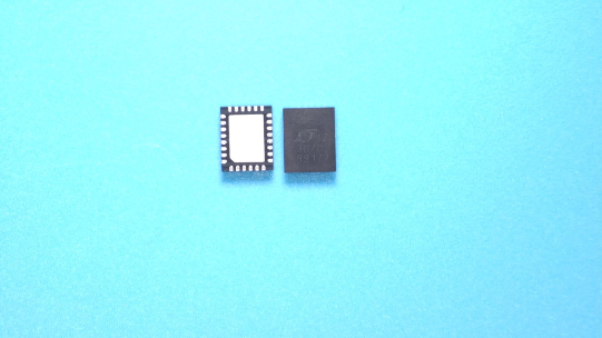
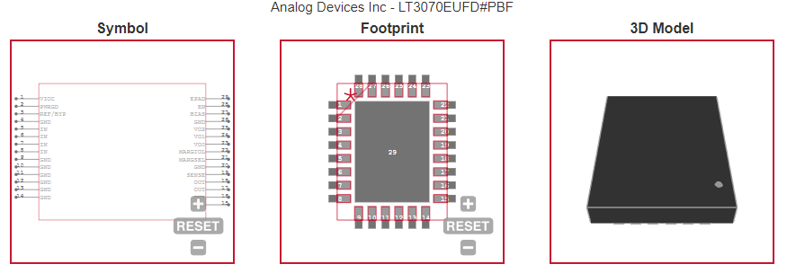
• 28-Lead (4mm × 5mm × 0.75mm) QFN Package
|
|
| CATALOG |
LT3070EUFD#PBF Country of Origin
|
LT3070EUFD#PBF Parametric Info
|
LT3070EUFD#PBF Package Info
|
LT3070EUFD#PBF Manufacturing Info
|
LT3070EUFD#PBF Packaging Info
|
LT3070EUFD#PBF ECAD Models
|
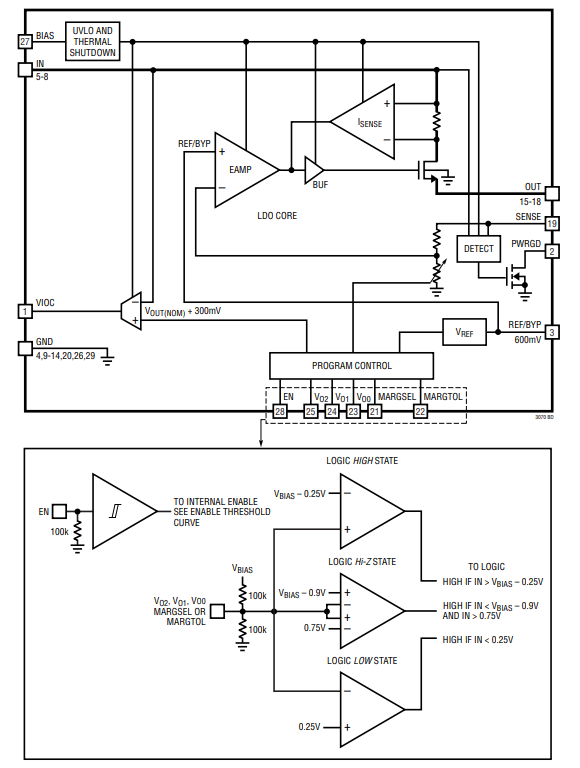
LT3070EUFD#PBF functional BLOCK DIAGRAM
|
LT3070EUFD#PBF APPLICATIONS
|
|
COUNTRY OF ORIGIN
|
Malaysia
|
|
PARAMETRIC INFO
|
| Type |
LDO |
| Number of Outputs |
1 |
| Maximum Output Current (A) |
5 |
| Minimum Operating Temperature (°C) |
-40 |
| Maximum Operating Temperature (°C) |
125 |
| Output Type |
Selectable |
| Output Voltage Range (V) |
<1.8|1.8 to 10 |
| Regulation Condition Change In Load |
4.99A |
| Regulation Condition Change In Line |
1.65V |
| Junction to Ambient |
35°C/W |
| Polarity |
Positive |
| Special Features |
Current Limit|Reverse Current Protection|Thermal Shutdown Protection |
| Load Regulation |
-7mV |
| Line Regulation |
1mV |
| Maximum Dropout Voltage @ Current (V) |
0.035@1A|0.065@2.5A|0.12@5A |
| Minimum Input Voltage (V) |
0.95 |
| Maximum Input Voltage (V) |
3 |
| Output Voltage (V) |
0.8 to 1.8 |
| Typical Dropout Voltage @ Current (V) |
0.02@1A|0.05@2.5A|0.085@5A |
| Accuracy (%) |
±1 |
| Supplier Temperature Grade |
Extended |
| Minimum Storage Temperature (°C) |
-65 |
| Maximum Storage Temperature (°C) |
150 |
| Typical Bias Voltage (VDC) |
2.2 to 3.6 |
| Typical PSRR (dB) |
75 |
| Typical Output Capacitance (uF) |
15(Min) |
| Typical Output Noise Voltage (uVrms) |
25 |
| Pass Element Type |
NMOS |
| Output Capacitor Type |
Ceramic |
|
|
PACKAGE INFO
|
| Supplier Package |
QFN EP |
| Basic Package Type |
Non-Lead-Frame SMT |
| Pin Count |
28 |
| Lead Shape |
No Lead |
| PCB |
28 |
| Tab |
N/R |
| Pin Pitch (mm) |
0.5 |
| Package Length (mm) |
5 |
| Package Width (mm) |
4 |
| Package Height (mm) |
0.75(Max) |
| Package Diameter (mm) |
N/R |
| Package Overall Length (mm) |
5 |
| Package Overall Width (mm) |
4 |
| Package Overall Height (mm) |
0.75 |
| Seated Plane Height (mm) |
0.75 |
| Mounting |
Surface Mount |
| Package Weight (g) |
N/A |
| Package Material |
Plastic |
| Package Description |
Quad Flat No Lead Package, Exposed Pad |
| Package Family Name |
QFN |
| Jedec |
MO-220WGHD-3 |
| Package Outline |
Link to Datasheet |
|
|
MANUFACTURING INFO
|
| MSL |
1 |
| Maximum Reflow Temperature (°C) |
260 |
| Reflow Solder Time (Sec) |
30 |
| Number of Reflow Cycle |
3 |
| Standard |
J-STD-020D |
| Reflow Temp. Source |
Link to Datasheet |
| Maximum Wave Temperature (°C) |
N/R |
| Wave Solder Time (Sec) |
N/R |
| Lead Finish(Plating) |
Matte Sn annealed |
| Under Plating Material |
Ag |
| Terminal Base Material |
Cu Alloy |
| Number of Wave Cycles |
N/R |
|
|
PACKAGING INFO
|
| Packaging |
Tube |
| Quantity Of Packaging |
73 |
|
|
ECAD MODELS
|
|
|
| FUNCTIONAL BLOCK DIAGRAM |
|
|
APPLICATIONS
|
• FPGA and DSP Supplies
|
• ASIC and Microprocessor Supplies
|
• Servers and Storage Devices
|
• Post Buck Regulation and Supply Isolation
|
|