|
| |
• Low Noise Voltage: 0.95nV/√Hz (100kHz)
|
• 5% Input Current Accuracy
|
• 200mA to 1000mA Program Range
|
| • Gain Bandwidth Product:LT6200/LT6201 165MHz AV = 1LT6200-5 800MHz AV ≥ 5LT6200-10 1.6GHz AV ≥ 10
|
| • Low Distortion: –80dB at 1MHz, RL = 100Ω |
| • Dual LT6201 in Tiny DFN Package |
| • Input Common Mode Range Includes Both Rails |
| • Output Swings Rail-to-Rail |
| • Low Offset Voltage: 1mV Max |
| • Wide Supply Range: 2.5V to 12.6V |
| • Output Current: 60mA Min |
| • Operating Temperature Range –40°C to 85°C |
| • Power Shutdown, Thermal Shutdown |
| • SO-8 and Low Profile (1mm) ThinSOT™ Packages |
| |
| CATALOG |
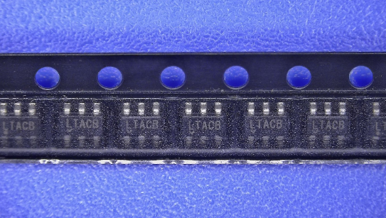
| LT6200IS6-5#TRMPBF COUNTRY OF ORIGIN |
LT6200IS6-5#TRMPBF PARAMETRIC INFO
|
LT6200IS6-5#TRMPBF PACKAGE INFO
|
LT6200IS6-5#TRMPBF MANUFACTURING INFO
|
LT6200IS6-5#TRMPBF PACKAGING INFO
|
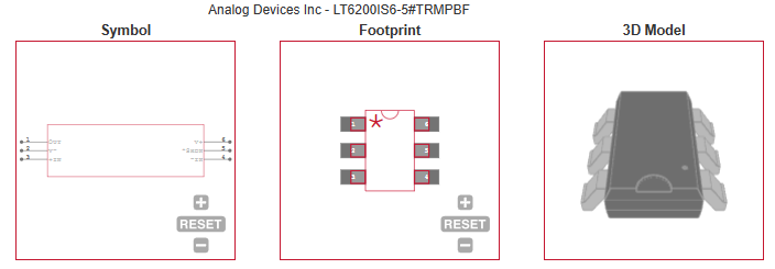
LT6200IS6-5#TRMPBF EACD MODELS
|
| LT6200IS6-5#TRMPBF APPLICATIONS |
|
| COUNTRY OF ORIGIN |
| Malaysia |
|
PARAMETRIC INFO
|
| Manufacturer Type |
Low Noise Amplifier |
| Type |
Low Noise Amplifier |
| Rail to Rail |
Rail to Rail Input/Output |
| Minimum Single Supply Voltage (V) |
2.5 |
| Number of Channels per Chip |
1 |
| Minimum PSRR (dB) |
60 |
| Typical Single Supply Voltage (V) |
3|5 |
| Maximum Single Supply Voltage (V) |
12.6 |
| Minimum Dual Supply Voltage (V) |
±1.25 |
| Typical Gain Bandwidth Product (MHz) |
750 |
| Maximum Input Offset Voltage (mV) |
2@5V |
| Typical Dual Supply Voltage (V) |
±5 |
| Maximum Input Offset Current (uA) |
5@5V |
| Maximum Dual Supply Voltage (V) |
±6.3 |
| Maximum Operating Supply Voltage (V) |
±6.3|12.6 |
| Maximum Input Bias Current (uA) |
18@5V |
| Minimum CMRR (dB) |
65 |
| Maximum Supply Voltage Range (V) |
12.5 to 15 |
| Minimum CMRR Range (dB) |
65 to 70 |
| Typical Voltage Gain (dB) |
101.58 |
| Typical Slew Rate (V/us) |
210@5V |
| Typical Input Offset Current (uA) |
0.4@5V |
| Minimum Slew Rate (V/us) |
31@5V |
| Typical Settling Time (ns) |
165 |
| Typical Output Current (mA) |
60(Min) |
| Typical Input Noise Voltage Density (nV/rtHz) |
1.5@5V |
| Typical Noninverting Input Current Noise Density (pA/rtHz) |
3.5@5V |
| Typical Input Bias Current (uA) |
8@5V |
| Shut Down Support |
Yes |
| Minimum Operating Temperature (°C) |
-40 |
| Maximum Operating Temperature (°C) |
85 |
| Supplier Temperature Grade |
Industrial |
| Minimum Storage Temperature (°C) |
-65 |
| Maximum Storage Temperature (°C) |
150 |
| Power Supply Type |
Single|Dual |
| Maximum Supply Current (mA) |
20@5V |
| Typical High Level Output Voltage (V) |
0.24 |
| Typical Low Level Output Voltage (V) |
0.16 |
| Input Offset Voltage Drift (uV/°C) |
8 |
|
|
PACKAGE INFO
|
| Supplier Package |
TSOT-23 |
| Basic Package Type |
Lead-Frame SMT |
| Pin Count |
6 |
| Lead Shape |
Gull-wing |
| PCB |
6 |
| Tab |
N/R |
| Pin Pitch (mm) |
0.95 |
| Package Length (mm) |
2.9 |
| Package Width (mm) |
1.75(Max) |
| Package Height (mm) |
0.9(Max) |
| Package Diameter (mm) |
N/R |
| Package Overall Length (mm) |
2.9 |
| Package Overall Width (mm) |
2.8 |
| Package Overall Height (mm) |
1(Max) |
| Seated Plane Height (mm) |
1(Max) |
| Mounting |
Surface Mount |
| Package Weight (g) |
N/A |
| Package Material |
Plastic |
| Package Description |
Thin Small Outline Transistor |
| Package Family Name |
SOT |
| Jedec |
MO-193AA |
| Package Outline |
Link to Datasheet |
|
|
MANUFACTURING INFO
|
| MSL |
1 |
| Maximum Reflow Temperature (°C) |
260 |
| Reflow Solder Time (Sec) |
30 |
| Number of Reflow Cycle |
3 |
| Standard |
J-STD-020D |
| Reflow Temp. Source |
Link to Datasheet |
| Maximum Wave Temperature (°C) |
260 |
| Wave Solder Time (Sec) |
10 |
| Wave Temp. Source |
Link to Datasheet |
| Lead Finish(Plating) |
Matte Sn annealed |
| Under Plating Material |
Ag |
| Terminal Base Material |
Cu Alloy |
|
|
PACKAGING INFO
|
| Packaging Suffix |
TRM |
| Packaging |
Tape and Reel |
| Quantity Of Packaging |
500 |
| Reel Diameter (in) |
7 |
| Reel Width (mm) |
8.4 |
| Tape Pitch (mm) |
4 |
| Tape Width (mm) |
8 |
| Feed Hole Pitch (mm) |
4 |
| Hole Center to Component Center (mm) |
2 |
| Component Orientation |
Q2 |
| Packaging Document |
Link to Datasheet |
|
|
ECAD MODELS
|
|
|
| APPLICATIONS |
| • Transimpedance Amplifiers |
| • Low Noise Signal Processing |
| • Active Filters |
| • Rail-to-Rail Buffer Amplifiers |
| • Driving A/D Converters |
|
| |