|
|
• Rail-to-Rail Input and Outputs
|
• Fast Settling Time: 240ns, 0.01%, 8VP-P Output Step
|
• 1.9nV/√Hz Input-Referred Op Amp Noise
|
| • High Impedance Input
|
| • –3dB Bandwidth: 33MHz |
| • 2.7V to 12V Supply Operation |
| • No External Gain Resistors Required |
| • 4.8mA Supply Current |
| • Low Power Shutdown |
| • Low Distortion (HD2/HD3): –102dBc/–97dBc at 100kHz, VOUTDIFF = 4VP-P |
| • Low Offset Voltage: ±400µV Max |
| • High DC Linearity: <±1LSB, 16-Bit, 8VP-P |
| • Low Input Current Noise: 1.1pA/√Hz |
| • 3mm × 3mm 8-Pin DFN and 8-Lead MSOP Packages |
|
| CATALOG |
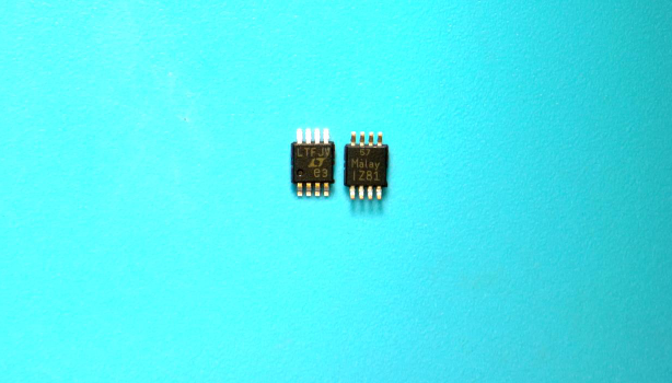
| LT6350CMS8#PBF COUNTRY OF ORIGIN |
LT6350CMS8#PBF PARAMETRIC INFO
|
LT6350CMS8#PBF PACKAGE INFO
|
LT6350CMS8#PBF MANUFACTURING INFO
|
LT6350CMS8#PBF PACKAGING INFO
|
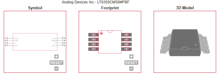
LT6350CMS8#PBF ECAD MODELS
|
| LT6350CMS8#PBF APPLICATIONS |
|
| COUNTRY OF ORIGIN |
| Malaysia |
|
PARAMETRIC INFO
|
| type |
Differential Amplifier |
| Rail to Rail |
Rail to Rail Input/Output |
| Number of Elements per Chip |
2 |
| Number of Channels per Chip |
2 |
| Output Type |
Differential |
| Minimum PSRR (dB) |
80 |
| Typical Gain Bandwidth Product (MHz) |
115 |
| Maximum Input Offset Voltage (mV) |
1.5@5V@0C to 70C |
| Maximum Input Bias Current (uA) |
8(Min)@5V@0C to 70C |
| Minimum CMRR (dB) |
82 |
| Minimum CMRR Range (dB) |
75 to 85 |
| Maximum Input Resistance (MOhm) |
4(Typ)@5V |
| Maximum Voltage Gain Range (dB) |
<35 |
| Maximum Voltage Gain (dB) |
6.02(Typ) |
| Minimum Operating Temperature (°C) |
0 |
| Maximum Operating Temperature (°C) |
70 |
| Supplier Temperature Rating |
Commercial |
| Minimum Storage Temperature (°C) |
-65 |
| Maximum Storage Temperature (°C) |
150 |
| Power Supply Type |
Single |
| Maximum Supply Voltage Range (V) |
10 to 15 |
| Minimum Single Supply Voltage (V) |
2.7 |
| Typical Single Supply Voltage (V) |
5 |
| Maximum Single Supply Voltage (V) |
12 |
| Maximum Operating Supply Voltage (V) |
12 |
| Maximum Supply Current (mA) |
5.8@5V |
|
|
PACKAGE INFO
|
| Supplier packaging |
MSOP |
| Basic package type |
Lead-Frame SMT |
| Number of pins |
8 |
| Pin shape |
Gull-wing |
| PCB |
8 |
| ears |
N/R |
| Pin spacing (mm) |
0.65 |
| Package length (mm) |
3 |
| Package width (mm) |
3 |
| Package height (mm) |
0.86 |
| Package diameter (mm) |
N/R |
| Package Overall Length (mm) |
3 |
| Package Overall Width (mm) |
4.9 |
| Package Overall Height (mm) |
1.1(Max) |
| Mounting surface height (mm) |
1.1(Max) |
| Install |
Surface Mount |
| Package weight (g) |
not applicable |
| Packaging materials |
Plastic |
| package instruction |
Micro Small Outline Package |
| Package series name |
SO |
| JEDEC |
MO-187AA |
| Package outline |
Link to datasheet |
|
|
MANUFACTURING INFO
|
| MSL |
1 |
| Maximum reflow temperature (°C) |
260 |
| Reflow soldering time (seconds) |
30 |
| Number of reflow cycles |
3 |
| standard |
J-STD-020D |
| Reflow temperature source |
Link to datasheet |
| Maximum wave soldering temperature (°C) |
260 |
| Wave soldering time (seconds) |
10 |
| Wave soldering temperature source |
Link to datasheet |
| Lead Finish(Plating) |
Matte Sn annealed |
| Plating materials |
Ag |
| Terminal Base Material |
Alloy 42 |
|
|
PACKAGING INFO
|
| Package |
Tube |
| Packing quantity |
50 |
|
|
ECAD MODELS
|
|
|
APPLICATIONS
|
• 16-Bit and 18-Bit SAR ADC Drivers
|
| • Single-Ended to Differential Conversion |
| • Differential Line Driver |
|
| |
| |