 |
|
| ■ Ultralow Quiescent Current: 2.1µA Typ (LTC1440)
|
| ■ Reference Output Drives 0.01µF Capacitor |
| ■ Adjustable Hysteresis (LTC1440/LTC1442) |
■ Wide Supply Range:
- Single: 2V to 11V
- Dual: ±1V to ±5.5V |
| ■ Input Voltage Range Includes the Negative Supply |
| ■ TTL/CMOS Compatible Outputs |
| ■ 12µs Propagation Delay with 10mV Overdrive |
| ■ No Crowbar Current |
| ■ 40mA Continuous Source Current |
| ■ Pin Compatible Upgrades for MAX921/922/923 |
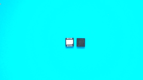
| ■ 3mm x 3mm x 0.75mm DFN Package (LTC1440)
|
|
| CATALOG |
| LTC1440IDD#PBF COUNTRY OF ORIGIN |
| LTC1440IDD#PBF PARAMETRIC INFO |
| LTC1440IDD#PBF PACKAGE INFO |
| LTC1440IDD#PBF MANUFACTURING INFO |
| LTC1440IDD#PBF PACKAGING INFO |
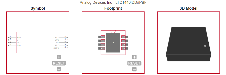
| LTC1440IDD#PBF ECAD MODELS |
| LTC1440IDD#PBF APPLICATIOS |
|
| COUNTRY OF ORIGIN |
| Malaysia |
| United States of America |
|
| PARAMETRIC INFO |
| Rail to Rail |
No |
| Manufacturer Type |
Ultra Low Power Comparator |
| Number of Channels per Chip |
1 |
| Typical PSRR (dB) |
80 |
| Output Type |
CMOS/TTL |
| Maximum Input Offset Voltage (mV) |
10@5V@-40C to 85C |
| Typical CMRR (dB) |
80 |
| Strobe Capability |
No |
| Typical Output Current (mA) |
0.02@5V |
| Maximum Propagation Delay Time (ns) |
15000(Typ) |
| Minimum Operating Temperature (°C) |
-40 |
| Maximum Operating Temperature (°C) |
85 |
| Minimum Storage Temperature (°C) |
-65 |
| Maximum Storage Temperature (°C) |
150 |
| Power Supply Type |
Single|Dual |
| Maximum Operating Supply Voltage (V) |
±5.5|11 |
| Minimum Single Supply Voltage (V) |
2 |
| Typical Single Supply Voltage (V) |
3|5|9 |
| Maximum Single Supply Voltage (V) |
11 |
| Minimum Dual Supply Voltage (V) |
±1 |
| Typical Dual Supply Voltage (V) |
±3|±5 |
| Maximum Dual Supply Voltage (V) |
±5.5 |
| Maximum Supply Current (mA) |
4.4@5V@-40C to 85C |
| Maximum Power Dissipation (mW) |
500 |
|
| |
| PACKAGE INFO |
| Supplier Package |
DFN EP |
| Basic Package Type |
Non-Lead-Frame SMT |
| Pin Count |
8 |
| Lead Shape |
No Lead |
| PCB |
8 |
| Tab |
N/R |
| Pin Pitch (mm) |
0.5 |
| Package Length (mm) |
3 |
| Package Width (mm) |
3 |
| Package Height (mm) |
0.75(Max) |
| Package Diameter (mm) |
N/R |
| Package Overall Length (mm) |
3 |
| Package Overall Width (mm) |
3 |
| Package Overall Height (mm) |
0.75 |
| Seated Plane Height (mm) |
0.75 |
| Mounting |
Surface Mount |
| Package Weight (g) |
N/A |
| Package Material |
Plastic |
| Package Description |
Dual Flat Package No Lead, Exposed Pad |
| Package Family Name |
DFN |
| Jedec |
MO-229 |
|
| |
| MANUFACTURING INFO |
| MSL |
1 |
| Maximum Reflow Temperature (°C) |
260 |
| Reflow Solder Time (Sec) |
30 |
| Number of Reflow Cycle |
3 |
| Standard |
J-STD-020D |
| Reflow Temp. Source |
Link to Datasheet |
| Maximum Wave Temperature (°C) |
N/R |
| Wave Solder Time (Sec) |
N/R |
| Lead Finish(Plating) |
Matte Sn annealed |
| Under Plating Material |
Ag |
| Terminal Base Material |
Cu Alloy |
|
| |
| PACKAGING INFO |
| Packaging |
Tube |
| Quantity Of Packaging |
121 |
|
| |
| ECAD MODELS |
 |
|
| APPLICATIOS |
| ■ Battery-Powered System Monitoring |
| ■ Threshold Detectors |
| ■ Window Comparators |
| ■ Oscillator Circuits |
|