|
|
• Two-Channel Simultaneously Sampling ADC
|
• 73.1dB SNR
|
• 90dB SFDR
|
• Low Power: 189mW/149mW/113mW Total 95mW/75mW/57mW per Channel
|
• Single 1.8V Supply
|
• CMOS, DDR CMOS, or DDR LVDS Outputs
|
• Selectable Input Ranges: 1VP-P to 2VP-P
|
|
| CATALOG |
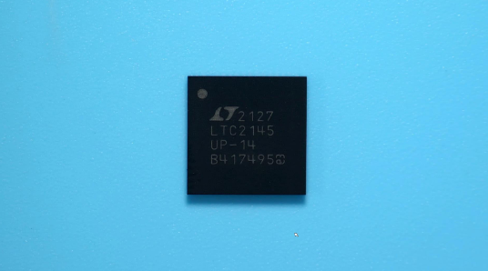
LTC2145IUP-14#PBF COUNTRY OF ORIGIN
|
LTC2145IUP-14#PBF PARAMETRIC INFO
|
LTC2145IUP-14#PBF PACKAGE INFO
|
LTC2145IUP-14#PBF MANUFACTURING INFO
|
LTC2145IUP-14#PBF PACKAGING INFO
|
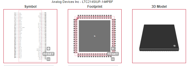
LTC2145IUP-14#PBF ECAD MODELS
|
LTC2145IUP-14#PBF APPLICATIONS
|
|
COUNTRY OF ORIGIN
|
Thailand
|
|
PARAMETRIC INFO
|
| Converter Type |
General Purpose |
| Input Type |
Voltage |
| Architecture |
Pipelined |
| Resolution |
14bit |
| Number of ADCs |
2 |
| Sampling Rate |
125Msps |
| Interface Type |
Parallel |
| Voltage Reference |
Internal|External |
| Input Signal Type |
Differential |
| Minimum Operating Temperature (°C) |
-40 |
| Maximum Operating Temperature (°C) |
85 |
| Supplier Temperature Grade |
Industrial |
| Minimum Storage Temperature (°C) |
-65 |
| Maximum Storage Temperature (°C) |
150 |
| Integral Nonlinearity Error |
±2.6LSB |
| Signal to Noise Ratio |
73.1dBFS(Typ) |
| Sample and Hold |
Yes |
| Number of Input Channels |
2 |
| Single-Ended Input |
No |
| Differential Input |
Yes |
| Input Voltage |
1Vp-p/2Vp-p |
| No Missing Codes (bit) |
14 |
| Full Scale Error |
-1.8/0.9%FSR |
| Differential Nonlinearity |
±0.9LSB |
| Voltage Supply Source |
Single |
| Minimum Single Supply Voltage (V) |
1.7 |
| Typical Single Supply Voltage (V) |
1.8 |
| Maximum Single Supply Voltage (V) |
1.9 |
| Digital Supply Support |
No |
| Typical Power Dissipation (mW) |
315 |
| Maximum Power Dissipation (mW) |
360 |
| Parallel Interface |
Parallel CMOS|Parallel LVDS |
|
|
PACKAGE INFO
|
| Supplier Package |
QFN EP |
| Basic Package Type |
Non-Lead-Frame SMT |
| Pin Count |
64 |
| Lead Shape |
No Lead |
| PCB |
64 |
| Tab |
N/R |
| Pin Pitch (mm) |
0.5 |
| Package Length (mm) |
9 |
| Package Width (mm) |
9 |
| Package Height (mm) |
0.75(Max) |
| Package Diameter (mm) |
N/R |
| Seated Plane Height (mm) |
0.75 |
| Mounting |
Surface Mount |
| Package Material |
Plastic |
| Package Description |
Quad Flat No Lead Package, Exposed Pad |
| Package Family Name |
QFN |
| Jedec |
N/A |
| Package Outline |
Link to Datasheet |
|
|
MANUFACTURING INFO
|
| MSL |
1 |
| Maximum Reflow Temperature (°C) |
260 |
| Reflow Solder Time (Sec) |
30 |
| Number of Reflow Cycle |
3 |
| Standard |
J-STD-020D |
| Reflow Temp. Source |
Link to Datasheet |
| Maximum Wave Temperature (°C) |
N/R |
| Wave Solder Time (Sec) |
N/R |
| Lead Finish(Plating) |
Matte Sn annealed |
| Under Plating Material |
Ag |
| Terminal Base Material |
Cu Alloy |
| Number of Wave Cycles |
N/R |
|
| |
| PACKAGING INFO |
| Packaging |
Tube |
| Quantity Of Packaging |
40 |
|
| |
| ECAD MODELS |
 |
|
| APPLICATIONS |
| • Communications |
| • Cellular Base Stations |
| • Software Defined Radios |
| • Portable Medical Imaging |
| • Multi-Channel Data Acquisition |
| • Nondestructive Testing |
| |