|
|
• Six Programmable Output Ranges:Unipolar: 0V to 5V, 0V to 10VBipolar: ±5V, ±10V, ±2.5V, –2.5V to 7.5V
|
• Serial Readback of All On-Chip Registers
|
• 1LSB INL and DNL Over the IndustrialTemperature Range (LTC2704-14/LTC2704-12)
|
• Force/Sense Outputs Enable Remote Sensing
|
• Glitch Impulse: < 2nV-sec
|
• Outputs Drive ±5mA
|
• Pin Compatible 12-, 14- and 16-Bit Parts
|
• Power-On and Clear to Zero Volts
|
• 44-Lead SSOP Package
|
|
| CATALOG |
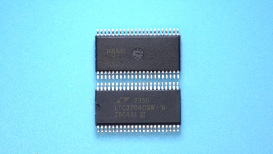
LTC2704CGW-16#PBF Country of Origin
|
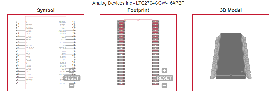
LTC2704CGW-16#PBF Parametric Info
|
LTC2704CGW-16#PBF Package Info
|
LTC2704CGW-16#PBF Manufacturing Info
|
LTC2704CGW-16#PBF Packaging Info
|
LTC2704CGW-16#PBF ECAD Models
|
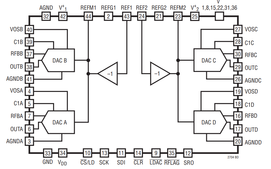
LTC2704CGW-16#PBF FUNCTIONAL BLOCK DIAGRAM
|
LTC2704CGW-16#PBF APPLICATIONS
|
|
COUNTRY OF ORIGIN
|
Malaysia
|
|
PARAMETRIC INFO
|
| C |
16bit |
| Number of DAC Channels |
4 |
| Number of Outputs per Chip |
4 |
| Converter Type |
General Purpose |
| Output Type |
Voltage |
| Voltage Reference |
External |
| Maximum Settling Time (us) |
10(Typ) |
| Digital Interface Type |
Serial (3-Wire, SPI) |
| Output Polarity |
Unipolar|Bipolar |
| Integral Nonlinearity Error |
±2LSB |
| Full Scale Error |
±20LSB |
| Minimum Operating Temperature (°C) |
0 |
| Maximum Operating Temperature (°C) |
70 |
| Power Supply Type |
Dual |
| Minimum Dual Supply Voltage (V) |
±4.5 |
| Typical Dual Supply Voltage (V) |
±15 |
| Maximum Dual Supply Voltage (V) |
±16.5 |
| Digital Supply Support |
Yes |
| Maximum Power Dissipation (mW) |
87.5(Typ) |
|
|
PACKAGE INFO
|
| Supplier Package |
SSOP W |
| Pin Count |
44 |
| PCB |
44 |
| Tab |
N/R |
| Pin Pitch (mm) |
0.8 |
| Package Length (mm) |
17.93(Max) |
| Package Width (mm) |
7.6(Max) |
| Package Height (mm) |
2.39(Max) |
| Package Diameter (mm) |
N/R |
| Seated Plane Height (mm) |
2.64(Max) |
| Mounting |
Surface Mount |
| Package Material |
Plastic |
| Package Description |
Shrink Small Outline Package Wide Body |
| Package Family Name |
SO |
| Package Outline |
Link to Datasheet |
|
|
MANUFACTURING INFO
|
| MSL |
3 |
| Maximum Reflow Temperature (°C) |
260 |
| Reflow Solder Time (Sec) |
30 |
| Number of Reflow Cycle |
3 |
| Standard |
J-STD-020D |
| Reflow Temp. Source |
Link to Datasheet |
| Maximum Wave Temperature (°C) |
260 |
| Wave Solder Time (Sec) |
10 |
| Wave Temp. Source |
Link to Datasheet |
| Lead Finish(Plating) |
Matte Sn annealed |
| Under Plating Material |
Ag |
| Terminal Base Material |
Cu Alloy |
|
|
PACKAGING INFO
|
| Packaging |
Tube |
| Quantity Of Packaging |
27 |
|
|
ECAD MODELS
|
|
|
| FUNCTIONAL BLOCK DIAGRAM |
|
|
APPLICATIONS
|
• Process Control and Industrial Automation
|
• Direct Digital Waveform Generation
|
• Software Controlled Gain Adjustment
|
• Automated Test Equipment
|
|
|