 |
|
| ■ Guaranteed Reset Assertion at VCC = 1V |
| ■ 1.5mA Maximum Supply Current |
| ■ SO-8 Packaging |
| ■ 4.65V Precision Voltage Monitor |
| ■ Power OK/Reset Time Delay: 200ms |
| ■ Minimum External Component Count |
| ■ Performance Specified Over Temperature |
| ■ Superior Upgrade for MAX699 |
|
| CATALOG |
| LTC699IS8#PBF COUNTRY OF ORIGIN |
| LTC699IS8#PBF PARAMETRIC INFO |
| LTC699IS8#PBF PACKAGE INFO |
| LTC699IS8#PBF MANUFACTURING INFO |
| LTC699IS8#PBF PACKAGING INFO |
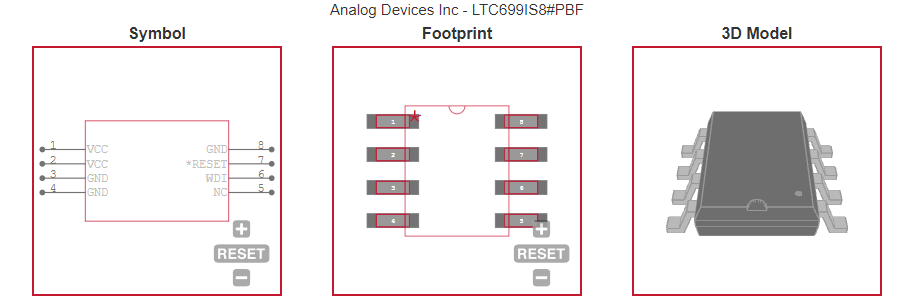
| LTC699IS8#PBF ECAD MODELS |
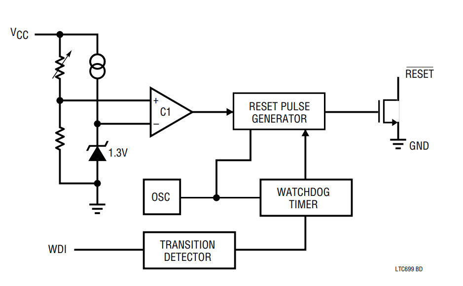
| LTC699IS8#PBF FUNCTIONAL BLOCK DIAGRAM |
| LTC699IS8#PBF APPLICATIONS |
|
| COUNTRY OF ORIGIN |
| Malaysia |
|
| PARAMETRIC INFO |
| Output Driver |
Active Low/Open Drain |
| Manual Reset |
No |
| Watchdog Timer |
Yes |
| Number of Supervisors |
1 |
| Typical Reset Threshold Voltage (V) |
4.65 |
| Minimum Operating Temperature (°C) |
-40 |
| Maximum Operating Temperature (°C) |
85 |
| Chip Enable Signals |
No |
| Power Fail Detection |
No |
| Battery Backup Switching |
No |
| Maximum Reset Active Time (ms) |
280 |
| Maximum Operating Supply Voltage (V) |
5.5 |
| Minimum Reset Threshold Voltage (V) |
4.5 |
| Maximum Reset Threshold Voltage (V) |
4.75 |
| Monitored Voltage (V) |
4.65 |
| Maximum Power Dissipation (mW) |
500 |
| Maximum Supply Current (uA) |
1500 |
| Minimum Operating Supply Voltage (V) |
3 |
| Supplier Temperature Grade |
Industrial |
| Type |
Power Supply Monitor |
|
| |
| PACKAGE INFO |
| Supplier Package |
SOIC N |
| Basic Package Type |
Lead-Frame SMT |
| Pin Count |
8 |
| Lead Shape |
Gull-wing |
| PCB |
8 |
| Tab |
N/R |
| Pin Pitch (mm) |
1.27 |
| Package Length (mm) |
5(Max) |
| Package Width (mm) |
3.99(Max) |
| Package Height (mm) |
1.5(Max) |
| Package Diameter (mm) |
N/R |
| Package Overall Length (mm) |
5(Max) |
| Package Overall Width (mm) |
6.2(Max) |
| Package Overall Height (mm) |
1.75(Max) |
| Seated Plane Height (mm) |
1.75(Max) |
| Mounting |
Surface Mount |
| Package Weight (g) |
N/A |
| Package Material |
Plastic |
| Package Description |
Small Outline IC Narrow Body |
| Package Family Name |
SO |
| Jedec |
MS-012AA |
| Package Outline |
Link to Datasheet |
|
| |
| MANUFACTURING INFO |
| MSL |
1 |
| Maximum Reflow Temperature (°C) |
260 |
| Reflow Solder Time (Sec) |
30 |
| Number of Reflow Cycle |
3 |
| Standard |
J-STD-020D |
| Reflow Temp. Source |
Link to Datasheet |
| Maximum Wave Temperature (°C) |
260 |
| Wave Solder Time (Sec) |
10 |
| Wave Temp. Source |
Link to Datasheet |
| Lead Finish(Plating) |
Matte Sn annealed |
| Under Plating Material |
Ag |
| Terminal Base Material |
Cu Alloy |
|
| |
| PACKAGING INFO |
| Packaging |
Tube |
| Quantity Of Packaging |
100 |
|
| |
| ECAD MODELS |
 |
|
| FUNCTIONAL BLOCK DIAGRAM |
 |
|
| APPLICATIONS |
| ■ Critical µP Power Monitoring |
| ■ Intelligent Instruments |
| ■ Computers and Controllers |
| ■ Automotive Systems |
|