 |
|
| • Complete Step-Down Switch Mode Power Supply
with Configurable Array of Five LDOs |
• Step-Down Switching Power Supply
- Adjustable 10% Accurate Output Current Limit
- Constant-Current, Constant-Voltage Operation
- Wide Input Voltage Range: 6V to 36V
- 1.2V to 24V Output Voltage |
• Configurable Output LDO Array
- Five 1.1A Parallelable Outputs
- Outputs Adjustable from 0V to 24V
- Low Output Noise: 90μVRMS (100Hz to 1MHz) |
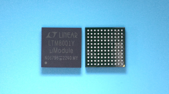
| • 15mm × 15mm × 3.42mm Surface Mount
BGA Packag |
|
| CATALOG |
| LTM8001IY#PBF COUNTRY OF ORIGIN |
| LTM8001IY#PBF PARAMETRIC INFO |
| LTM8001IY#PBF PACKAGE INFO |
| LTM8001IY#PBF MANUFACTURING INFO |
| LTM8001IY#PBF PACKAGING INFO |
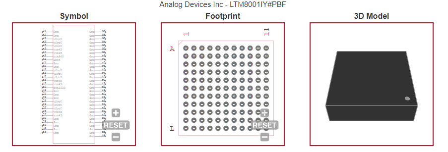
| LTM8001IY#PBF ECAD MODELS |
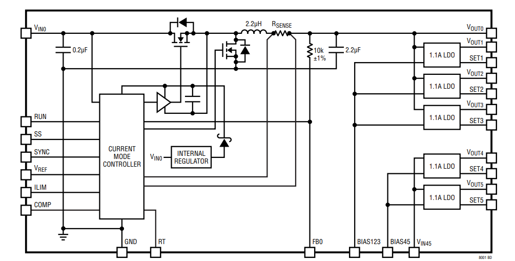
| LTM8001IY#PBF FUNCYIONAL BLOCK DIAGRAM |
| LTM8001IY#PBF APPLICATIONS |
|
| COUNTRY OF ORIGIN |
| Korea (Republic of) |
| Malaysia |
| United States of America |
|
| PARAMETRIC INFO |
| Isolation |
Non-Isolated |
| Type |
Step Down |
| Number of Outputs |
1 |
| Output Voltage (V) |
1.2 to 24 |
| Maximum Output Current (A) |
5 |
| Minimum Operating Temperature (°C) |
-40 |
| Maximum Operating Temperature (°C) |
125 |
| Supplier Temperature Grade |
Industrial |
| Switching Regulator |
Yes |
| Minimum Input Voltage (V) |
6 |
| Maximum Input Voltage (V) |
36 |
| Output Type |
Adjustable |
| Load Regulation |
1.2%(Typ) |
| Line Regulation |
0.5%(Typ) |
| Switching Frequency (kHz) |
1000(Typ) |
| Typical Standby Current (mA) |
0 |
| Minimum Storage Temperature (°C) |
-55 |
| Maximum Storage Temperature (°C) |
125 |
| On/Off Logic |
Positive |
|
| |
| PACKAGE INFO |
| Supplier Package |
BGA |
| Basic Package Type |
Ball Grid Array |
| Pin Count |
121 |
| Lead Shape |
Ball |
| PCB |
121 |
| Tab |
N/R |
| Pin Pitch (mm) |
1.27 |
| Package Length (mm) |
15 |
| Package Width (mm) |
15 |
| Package Height (mm) |
2.82 |
| Package Diameter (mm) |
N/R |
| Package Overall Length (mm) |
15 |
| Package Overall Width (mm) |
15 |
| Package Overall Height (mm) |
3.42 |
| Seated Plane Height (mm) |
3.42 |
| Mounting |
Surface Mount |
| Package Material |
Plastic |
| Package Description |
Plastic Ball Grid Array |
| Package Family Name |
BGA |
| Jedec |
MS-034BAE-1 |
| Package Outline |
Link to Datasheet |
|
| |
| MANUFACTURING INFO |
| MSL |
3 |
| Maximum Reflow Temperature (°C) |
245 |
| Reflow Solder Time (Sec) |
30 |
| Number of Reflow Cycle |
3 |
| Standard |
J-STD-020D |
| Reflow Temp. Source |
Link to Datasheet |
| Maximum Wave Temperature (°C) |
260 |
| Wave Solder Time (Sec) |
10 |
| Wave Temp. Source |
Link to Datasheet |
| Lead Finish(Plating) |
SnAgCu |
| Under Plating Material |
N/A |
| Terminal Base Material |
N/A |
|
| |
| PACKAGING INFO |
| Packaging |
Tray |
| Quantity Of Packaging |
119 |
|
| |
| ECAD MODELS |
 |
|
| FUNCYIONAL BLOCK DIAGRAM |
 |
|
| APPLICATIONS |
| • FPGA, DSP, ASIC and Microprocessor Supplies |
| • Servers and Storage Devices |
| • RF Transceivers |
|