|
|
• SUPPLY VOLTAGE
– VCC = 2.7V to 3.6V for Program, Erase
and Read
– VPP =12V for Fast Program (optional)
|
• ACCESS TIME: 70ns
|
• PROGRAMMING TIME
– 10µs per Byte/Word typical
– Double Word/ Quadruple Byte Program
|
• MEMORY BLOCKS
– Dual Bank Memory Array: 8Mbit+24Mbit
– Parameter Blocks (Top or Bottom
Location)
|
• ERASE SUSPEND and RESUME MODES
– Read and Program another Block during
Erase Suspend
|
| • UNLOCK BYPASS PROGRAM COMMAND
– Faster Production/Batch Programming |
| • VPP/WP PIN for FAST PROGRAM and
WRITE PROTECT |
| • TEMPORARY BLOCK UNPROTECTION
MODE |
| •COMMON FLASH INTERFACE
– 64 bit Security Code |
| • EXTENDED MEMORY BLOCK
– Extra block used as security block or to
store additional information |
| • LOW POWER CONSUMPTION
– Standby and Automatic Standby |
| • 100,000 PROGRAM/ERASE CYCLES per
BLOCK |
| • ELECTRONIC SIGNATURE
– Manufacturer Code: 0020h
– Top Device Code M29DW323DT: 225Eh
– Bottom Device Code M29DW323DB:
225Fh |
|
| CATALOG |
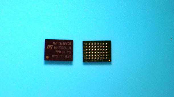
M29DW323DB70ZE6E COUNTRY OF ORIGIN
|
M29DW323DB70ZE6E PARAMETRIC INFO
|
M29DW323DB70ZE6E PACKAGE INFO
|
M29DW323DB70ZE6E MANUFACTURING INFO
|
M29DW323DB70ZE6E PACKAGING INFO
|
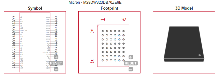
M29DW323DB70ZE6E ECAD MODELS
|
|
COUNTRY OF ORIGIN
|
Malaysia
|
|
PARAMETRIC INFO
|
| Density (bit) |
32M |
| Cell Type |
NOR |
| Interface Type |
Parallel |
| Block Organization |
Asymmetrical |
| Boot Block |
Yes |
| Timing Type |
Asynchronous |
| Architecture |
Sectored |
| Maximum Access Time (ns) |
70 |
| Typical Operating Supply Voltage (V) |
3|3.3 |
| Programmability |
Yes |
| Minimum Operating Temperature (°C) |
-40 |
| Maximum Operating Temperature (°C) |
85 |
| Supplier Temperature Grade |
Automotive |
| Number of Bits per Word (bit) |
8/16 |
| Number of Words |
4M/2M |
| Location of Boot Block |
Bottom |
| Maximum Operating Current (mA) |
10 |
| Programming Voltage (V) |
11.5 to 12.5 |
| Sector Size |
8Kbyte x 8|64Kbyte x 63 |
| OE Access Time (ns) |
30 |
| Program Current (mA) |
20 |
| Address Bus Width (bit) |
22/21 |
| Bank Size |
8/24Mb |
| Number of Banks |
2 |
| Minimum Operating Supply Voltage (V) |
2.7 |
| Maximum Operating Supply Voltage (V) |
3.6 |
| Maximum Erase Time (s) |
200/Chip |
| Maximum Programming Time (ms) |
200000/Chip |
| Command Compatible |
Yes |
| ECC Support |
No |
| Erase Suspend/Resume Modes Support |
Yes |
| Simultaneous Read/Write Support |
No |
| Support of Common Flash Interface |
Yes |
| Support of Page Mode |
No |
| Minimum Endurance (Cycles) |
100000 |
| Minimum Storage Temperature (°C) |
-65 |
| Maximum Storage Temperature (°C) |
150 |
| Density in Bits (bit) |
33554432 |
|
|
PACKAGE INFO
|
| Supplier Package |
TFBGA |
| Basic Package Type |
Ball Grid Array |
| Pin Count |
48 |
| Lead Shape |
Ball |
| PCB |
48 |
| Tab |
N/R |
| Pin Pitch (mm) |
0.8 |
| Package Length (mm) |
8 |
| Package Width (mm) |
6 |
| Package Height (mm) |
0.9(Max) |
| Package Diameter (mm) |
N/R |
| Seated Plane Height (mm) |
1.2(Max) |
| Mounting |
Surface Mount |
| Package Material |
Plastic |
| Package Description |
Thin Fine Pitch Ball Grid Array |
| Package Family Name |
BGA |
| Jedec |
N/A |
|
|
MANUFACTURING INFO
|
| MSL |
3 |
| Maximum Reflow Temperature (°C) |
260 |
| Reflow Solder Time (Sec) |
30 |
| Number of Reflow Cycle |
3 |
| Standard |
J-STD-020D |
| Maximum Wave Temperature (°C) |
N/R |
| Wave Solder Time (Sec) |
N/R |
| Lead Finish(Plating) |
SnAgCu |
| Under Plating Material |
N/A |
| Terminal Base Material |
N/A |
|
|
PACKAGING INFO
|
| Packaging Suffix |
E |
| Packaging |
Tray |
|
|
ECAD MODELS
|
|
|
| |