|
| |
• Designed for 2.0 V to 5.5 V VCC Operation
|
• 3.5 ns tPD at 5 V (typ)
|
• Inputs/Outputs Over−Voltage Tolerant up to 5.5 V
|
| • IOFF Supports Partial Power Down Protection |
| • Source/Sink 8 mA at 3.0 V |
| • Available in SC−88A, SC−74A, TSOP−5, SOT−953 and UDFN6 Packages |
| • Chip Complexity < 100 FETs |
| |
| CATALOG |
| M74VHC1GT08DFT2G COUNTRY OF ORIGIN |
| M74VHC1GT08DFT2G LIFECYCLE |
M74VHC1GT08DFT2G PARAMETRIC INFO
|
M74VHC1GT08DFT2G PACKAGE INFO
|
M74VHC1GT08DFT2G MANUFACTURING INFO
|
M74VHC1GT08DFT2G PACKAGING INFO
|
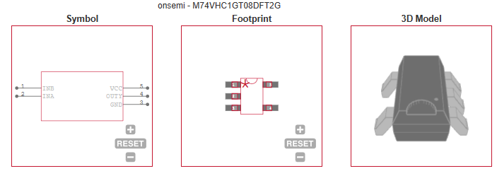
M74VHC1GT08DFT2G EACD MODELS
|
|
| COUNTRY OF ORIGIN |
| China |
| United States of America |
| Malaysia |
|
| LIFECYCLE |
Obsolete
Nov 20,2023 |
| |
PARAMETRIC INFO
|
| Logic Family |
VHC |
| Logic Function |
AND |
| Number of Element Inputs |
2-IN |
| Number of Element Outputs |
1 |
| Maximum Supply Current (mA) |
50 |
| Number of Elements per Chip |
1 |
| Number of Output Enables per Element |
0 |
| Number of Selection Inputs per Element |
0 |
| Process Technology |
CMOS |
| Minimum Operating Supply Voltage (V) |
2 |
| Maximum Operating Supply Voltage (V) |
5.5 |
| Typical Operating Supply Voltage (V) |
2.5|3.3|5 |
| Maximum High Level Output Current (mA) |
-8 |
| Maximum Low Level Output Current (mA) |
8 |
| Minimum Operating Temperature (°C) |
-55 |
| Maximum Operating Temperature (°C) |
125 |
| Minimum Storage Temperature (°C) |
-65 |
| Maximum Storage Temperature (°C) |
150 |
| Maximum Propagation Delay Time @ Maximum CL (ns) |
12.3@3V to 3.6V|7.9@4.5V to 5.5V |
| Absolute Propagation Delay Time (ns) |
16.5 |
| Propagation Delay Test Condition (pF) |
50 |
| Maximum Quiescent Current (uA) |
1 |
|
|
PACKAGE INFO
|
| Supplier Package |
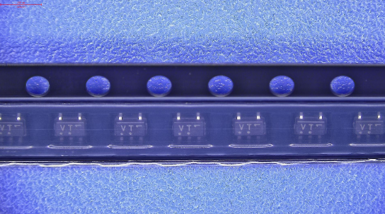
SC-88A |
| Basic Package Type |
Lead-Frame SMT |
| Pin Count |
5 |
| Lead Shape |
Gull-wing |
| PCB |
5 |
| Tab |
N/R |
| Pin Pitch (mm) |
0.65 |
| Package Length (mm) |
2.2(Max) |
| Package Width (mm) |
1.35(Max) |
| Package Height (mm) |
1(Max) |
| Package Diameter (mm) |
N/R |
| Package Overall Length (mm) |
2.2(Max) |
| Package Overall Width (mm) |
2.2(Max) |
| Package Overall Height (mm) |
1.1(Max) |
| Seated Plane Height (mm) |
1.1(Max) |
| Mounting |
Surface Mount |
| Package Weight (g) |
N/A |
| Package Material |
Plastic |
| Package Description |
Small Outline Transistor |
| Package Family Name |
SOT |
| Jedec |
N/A |
| Package Outline |
Link to Datasheet |
|
|
MANUFACTURING INFO
|
| MSL |
1 |
| Maximum Reflow Temperature (°C) |
260 |
| Reflow Solder Time (Sec) |
20 to 40 |
| Number of Reflow Cycle |
3 |
| Standard |
J-STD-020C |
| Reflow Temp. Source |
Link to Datasheet |
| Maximum Wave Temperature (°C) |
N/R |
| Wave Solder Time (Sec) |
N/R |
| Lead Finish(Plating) |
Matte Sn annealed |
| Under Plating Material |
N/A |
| Terminal Base Material |
FeNi Alloy |
|
|
PACKAGING INFO
|
| Packaging Suffix |
T2 |
| Packaging |
Tape and Reel |
| Quantity Of Packaging |
3000 |
| Packaging Document |
Link to Datasheet |
|
|
ECAD MODELS
|
|
|
| |