|
| |
• Robust Galvanic Isolation of Digital Signals• Withstands up to 2.75kVRMS for 60s (VISO)(MAX14930–MAX14932)• Continuously Withstands 443VRMS (VIOWM)(MAX14930–MAX14932)• 630VPK Repetitive Peak Voltage (VIORM)(MAX14930–MAX14932)• Withstands ±10kV Surge per IEC 61000-4-5
|
• Interfaces Directly with Most Micros and FPGAs• Accepts 1.71V to 5.5V Supplies
|
• Many Options Support Broad Applications• 3 Data Rates (1Mbps, 25Mbps, 150Mbps)• 3 Channel Direction Configuration• 2 Output Default States (High or Low)• 3 Packages (4mm, 8mm Creepage and Clearance)
|
• Low Power Consumption at High Data Rates At 1.8V:• 2.5mA per Channel Typical at 1Mbps• 5.25mA per Channel Typical at 100Mbps
At 3.3V:• 2.6mA per Channel Typical at 1Mbps• 7.1mA per Channel Typical at 100Mbps |
|
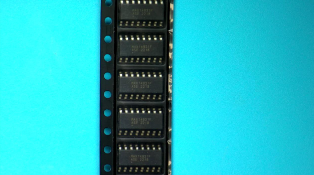
| CATALOG |
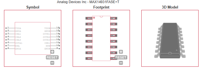
MAX14931FASE+T PARAMETRIC INFO
|
MAX14931FASE+T PACKAGE INFO
|
MAX14931FASE+T MANUFACTURING INFO
|
MAX14931FASE+T PACKAGING INFO
|
MAX14931FASE+T EACD MODELS
|
| MAX14931FASE+T APPLICATIONS |
|
PARAMETRIC INFO
|
| Number of Channels per Chip |
4 |
| Type |
SPI|I2C |
| Isolated Power |
No |
| Output Type |
CMOS |
| Minimum Isolation Voltage (Vrms) |
2750 |
| Maximum Power Dissipation (mW) |
1066.7 |
| Minimum Pulse Width (ns) |
40 |
| Maximum Pulse Width Distortion (ns) |
4.7 |
| Minimum Common Mode Rejection (kV/us) |
25(Typ) |
| Maximum Fall Time (ns) |
2 |
| Maximum Rise Time (ns) |
2 |
| Maximum Propagation Delay Time (tPHL) (ns) |
60.2 |
| Maximum Propagation Delay Time (tPLH) (ns) |
58.4 |
| Maximum Data Rate |
150Mbps |
| Minimum Operating Supply Voltage (V) |
1.71 |
| Maximum Operating Supply Voltage (V) |
5.5 |
| Minimum Operating Temperature (°C) |
-40 |
| Maximum Operating Temperature (°C) |
125 |
| Coupling Type |
Capacitive Coupling |
| Forward/Reverse Channels |
3/1 |
| Process Technology |
BiCMOS |
| Minimum Storage Temperature (°C) |
-65 |
| Maximum Storage Temperature (°C) |
150 |
|
|
PACKAGE INFO
|
| Supplier Package |
SOIC N |
| Basic Package Type |
Lead-Frame SMT |
| Pin Count |
16 |
| Lead Shape |
Gull-wing |
| PCB |
16 |
| Tab |
N/R |
| Pin Pitch (mm) |
1.27 |
| Package Length (mm) |
9.9 |
| Package Width (mm) |
3.9 |
| Package Height (mm) |
1.37 |
| Package Diameter (mm) |
N/R |
| Package Overall Length (mm) |
9.9 |
| Package Overall Width (mm) |
6 |
| Package Overall Height (mm) |
1.55 |
| Seated Plane Height (mm) |
1.55 |
| Mounting |
Surface Mount |
| Package Weight (g) |
N/A |
| Package Material |
Plastic |
| Package Description |
Small Outline IC Narrow Body |
| Package Family Name |
SO |
| Jedec |
MS-012AC |
| Package Outline |
Link to Datasheet |
|
|
MANUFACTURING INFO
|
| MSL |
1 |
| Maximum Reflow Temperature (°C) |
260 |
| Reflow Solder Time (Sec) |
30 |
| Number of Reflow Cycle |
3 |
| Standard |
J-STD-020D |
| Reflow Temp. Source |
Link to Datasheet |
| Maximum Wave Temperature (°C) |
N/R |
| Wave Solder Time (Sec) |
N/R |
| Wave Temp. Source |
Link to Datasheet |
| Lead Finish(Plating) |
Matte Sn annealed |
| Under Plating Material |
N/A |
| Terminal Base Material |
N/A |
| Number of Wave Cycles |
N/R |
|
|
PACKAGING INFO
|
| Packaging Suffix |
T |
| Packaging |
Tape and Reel |
| Quantity Of Packaging |
2500 |
| Reel Diameter (in) |
13 |
| Tape Pitch (mm) |
12 |
| Tape Width (mm) |
16 |
| Component Orientation |
Q1 |
| Packaging Document |
Link to Datasheet |
|
|
ECAD MODELS
|
|
|
| APPLICATIONS |
| • Fieldbus Communications for Industrial Automation |
| • Isolated SPI, RS-232, RS-485/RS-422 |
| • General Multichannel Isolation Applications |
| • Battery Management |
| • Medical Systems |
| |